January 31, 2023
Exploring Different Types of Vias in PCB
Share

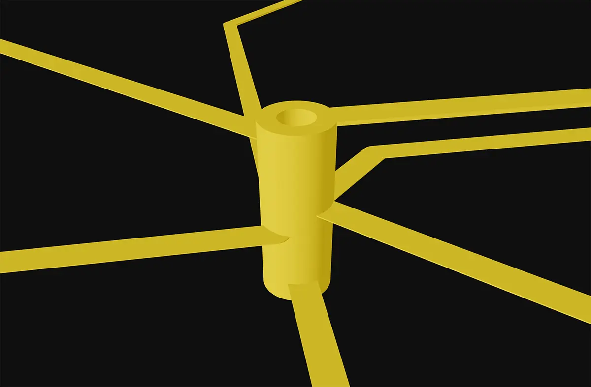
Through-hole vias are the most common type of vias used in PCBs. They are created by drilling a hole through the PCB and filling it with a conductive material, such as copper. These vias are typically used to connect the components to the other layers of the board and to provide structural support. Though-hole vias are drilled from the PCB's top layer to the bottom layer. When you look at a printed circuit board and look at it directly facing the light, the holes where light passes through are the through-hole vias.

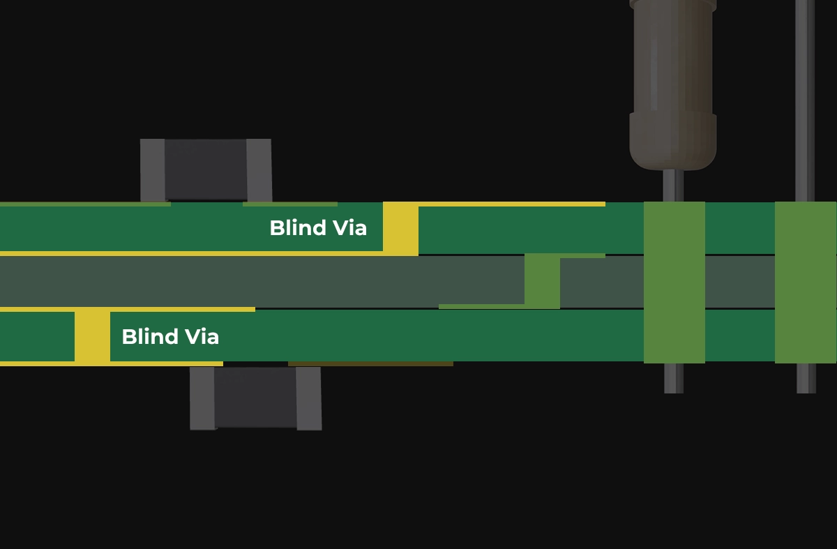
Blind vias are similar to through-hole vias, but only extend partially through the board. They connect an exterior copper layer to an interior later without reaching the other side of the board. This type of vias is ideal for multi-layer PCBs where space is limited.
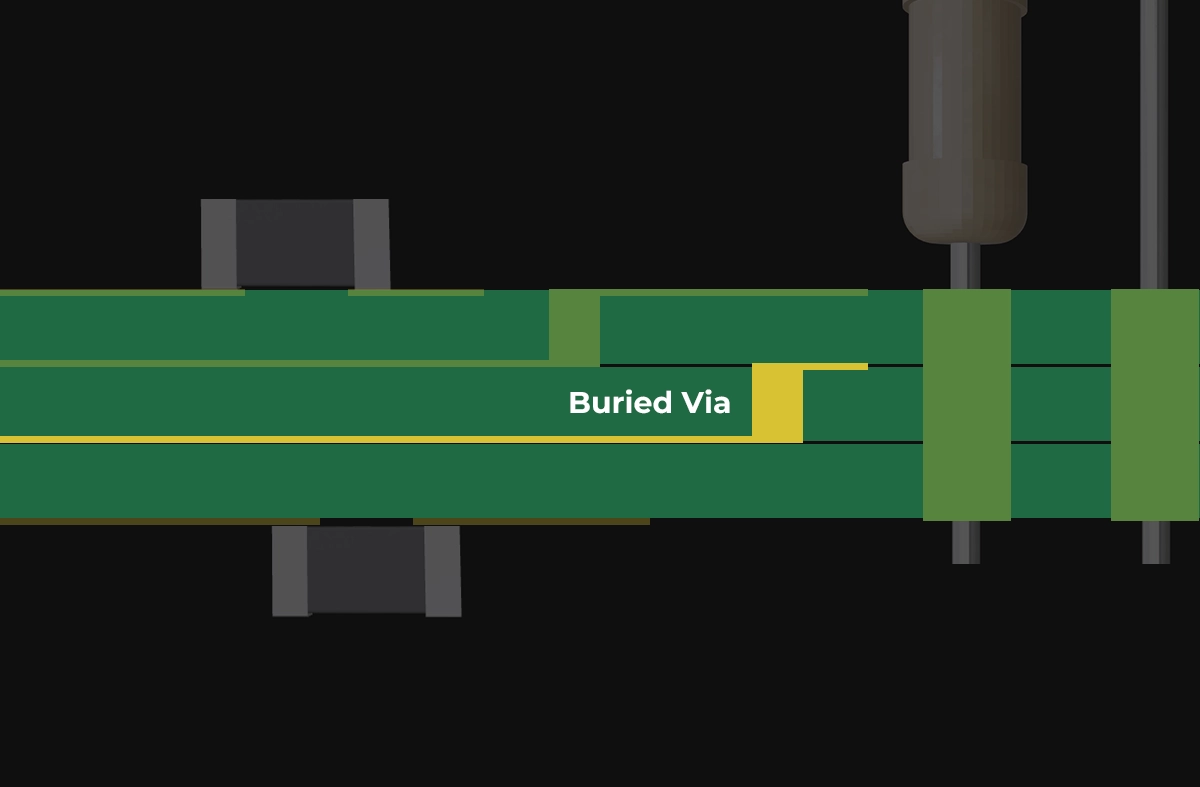
Buried vias are a type of blind vias that are completely hidden within the layers of the PCB. They connect two or more interior copper layers of the board. This type of vias is ideal for high-density PCBs where space is a premium.
Micro vias are very small vias that are used in high-density PCBs where space is limited. They are used to connect the internal layers of the board and are typically has a maximum of 0.15mm in diameter, maximum aspect ratio of 1:1, maximum depth of 0.25mm. Micro vias are ideal for high-speed signals and are commonly used in cell phones and other compact electronics.
In conclusion, there are several types of PCB vias, each with its own unique set of applications. Through-hole vias are the most common type of vias and cheaper to manufacture, while blind vias, buried vias, and micro vias are used in specific applications where space and performance are a concern. Understanding the different types of vias and their applications is crucial for designing and manufacturing high-quality PCBs.


Learn about STM32 microcontrollers, popular series, USB OTG, SWD, UART, and development tools. Find the right STM32 MCU and kickstart your projects.
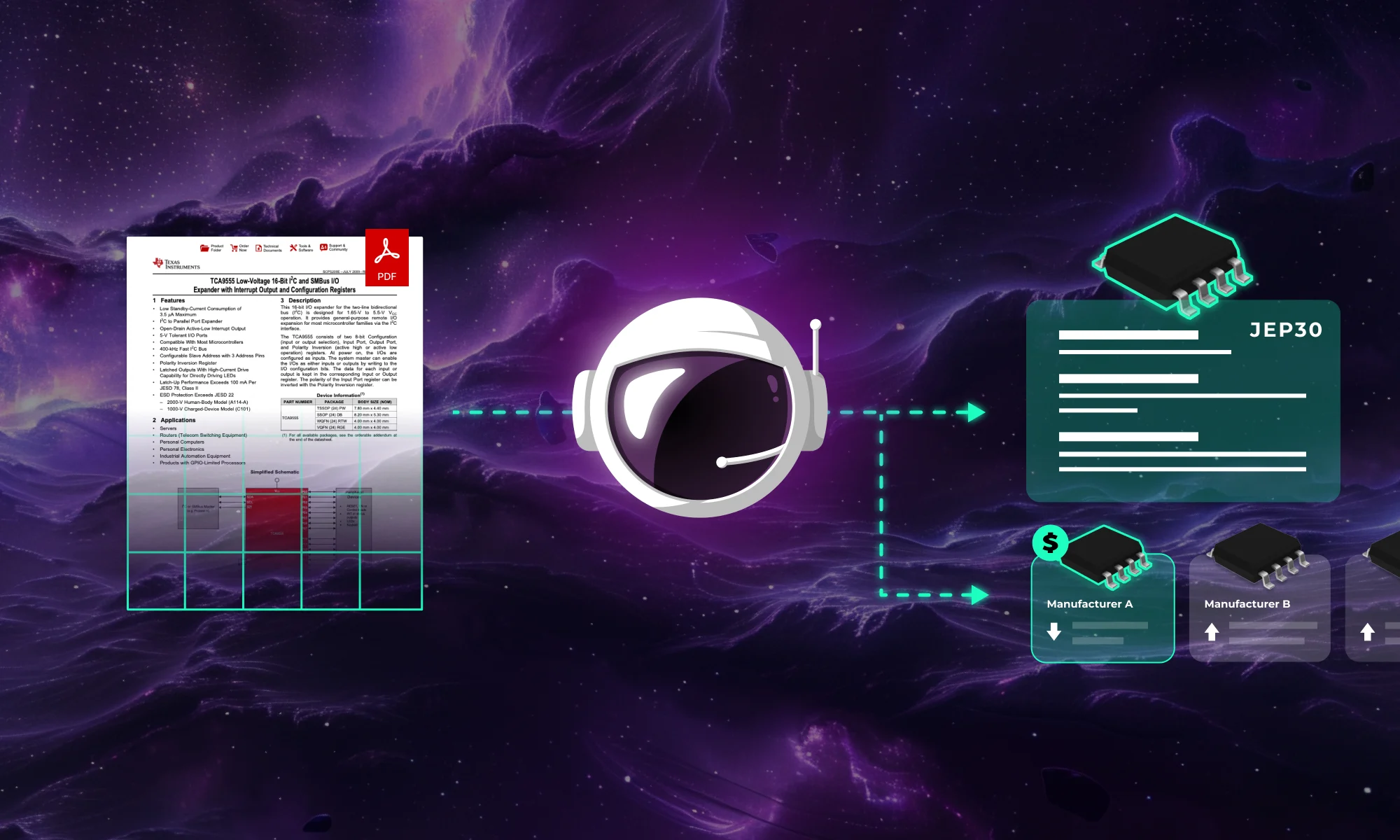
Discover how CAD Librarians can leverage Flux’s key capabilities—AI Part Imports, Component Updates, Live Pricing, and JEP30 Export—each tailored to meet the specific demands of maintaining PCB libraries.

Despite newer technologies like USB and Ethernet, RS232 remains widely used due to its simplicity and broad compatibility. It's crucial in industries, scientific instruments, networking gear, and legacy computers. This protocol's reliability makes it the go-to for many applications. In this blog, we'll explore why RS232 continues to be relevant in our tech-savvy world.
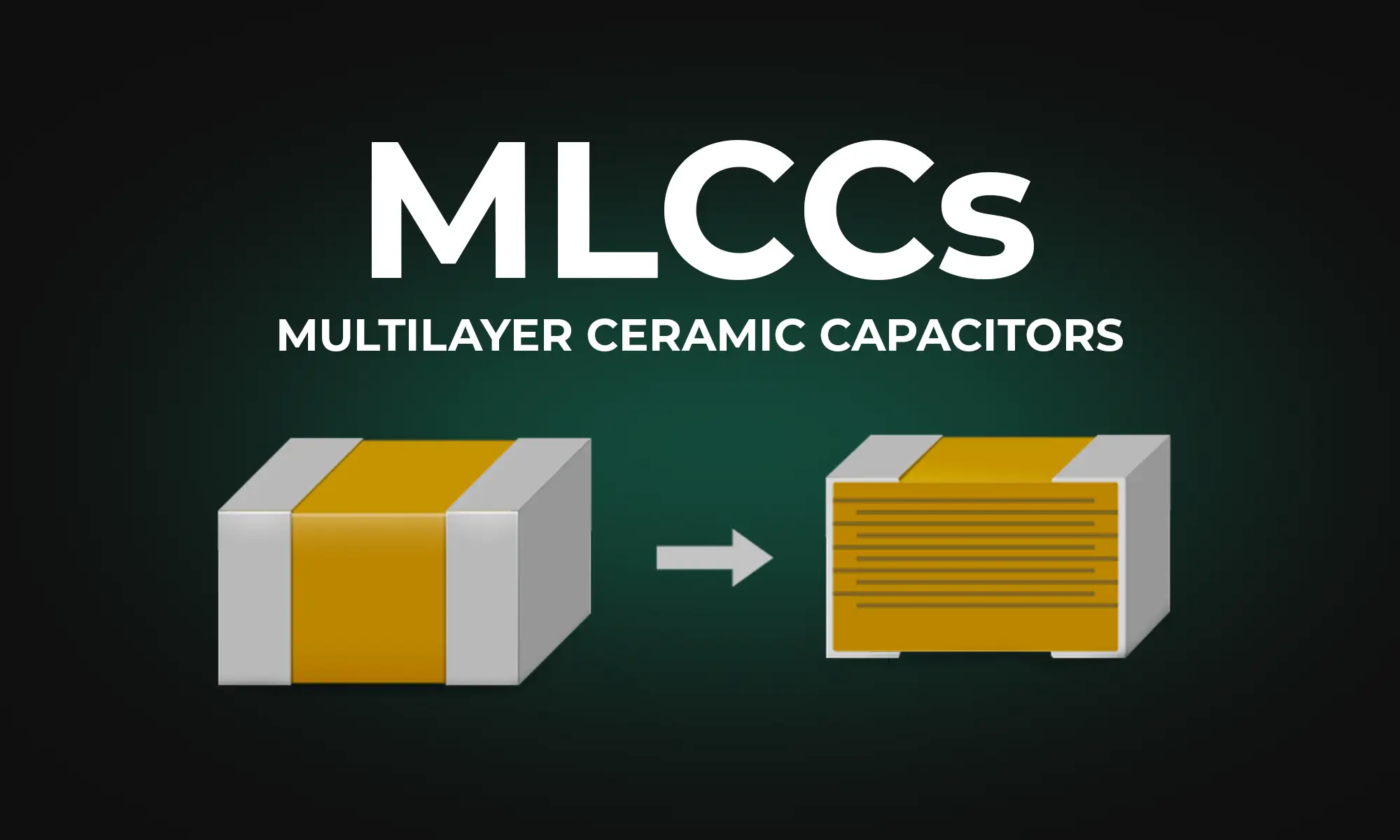
The blog post dives into the technical aspects of Multilayer Ceramic Capacitors (MLCCs), highlighting their importance in electronic circuits. It explains the construction of MLCCs, where layers of ceramic material and metal electrodes create a multilayered structure to store electrical energy.
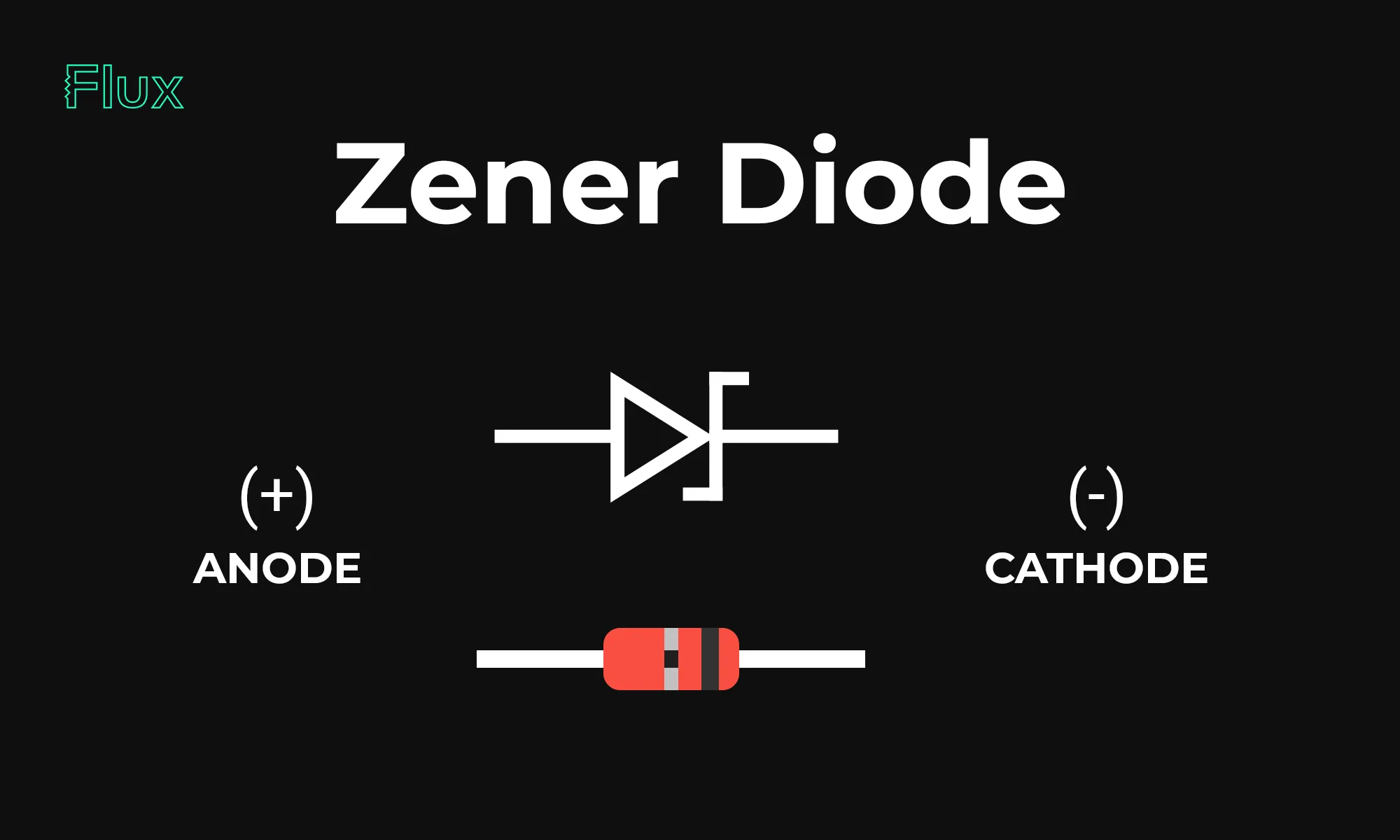
The blog offers an in-depth look at Zener diodes, highlighting their crucial role in voltage regulation and stability in electronic circuits. It covers their basic principles, applications, and the challenges faced in their usage.
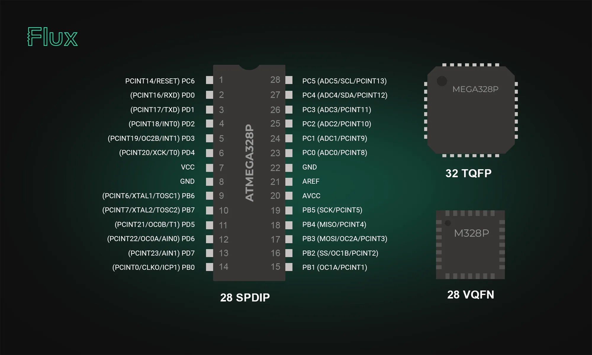
The ATmega328p stands out in the microcontroller world; our post breaks down its datasheet and pinout, offering valuable insights into its functionality and versatility. Learn how this powerful microcontroller can enhance your projects.

Looking for a comprehensive guide to ESP8266 pinout? Check out our article that covers everything you need to know about the ESP8266's pins, including digital, analog, and PWM pins. Perfect for beginners and experts alike, our guide will help you understand the ESP8266's pinout and how to use it in your projects.

Think you're familiar with the push button and its symbol? Prepare to be surprised! Join us in our latest blog post where we unravel the intricate science behind every press, click, and circuit, revealing the complexities hidden in the simplicity of a push button switch.
