July 24, 2023
Designing PCBs: What Are the Essential Steps
Share

A PCB, or Printed Circuit Board, is a mechanically designed structure that electrically connects and mechanically supports electronic components using conductive tracks, pads, and other features etched from copper layers laminated onto a non-conductive substrate.
PCBs play a pivotal role in the functionality of virtually all electronic devices. They provide a physical platform for mounting components and establish the necessary electrical interconnections, thus forming a system's electronic circuitry.
The purpose of this article is to demystify the process of PCB design, taking you through the essential steps from conception to completion, along with offering practical tips for success.
The basis of any printed circuit board design lies in the electronic circuit you aim to build. Thus, a firm grasp of circuit design principles, such as understanding how different components interact and basic electronic principles, is vital.
Before starting the design, it is crucial to define the design parameters. These could include the board's size and shape, the number of layers, the types of components used (through-hole or surface mount), the operating environment, power requirements, and more.
Based on the design parameters and functional requirements, the right components and board material (such as dielectric) must be selected. Components should be chosen based on electrical requirements, availability, cost, and space considerations, while board material should provide appropriate thermal and mechanical stability.
The first step in PCB design is creating a schematic diagram that represents the electrical connections between different components. It serves as a blueprint for the PCB layout.
Each component symbol is placed on the schematic, and interconnections are drawn using lines to represent electrical connections or nets. Different components like resistors, capacitors, transistors, inductors, and integrated circuits, will each have their own unique component symbol.
The completed schematic diagram is used to generate a netlist, which is a comprehensive report detailing every electrical connection in the design.
Before progressing, the schematic should be thoroughly checked for errors to prevent problems in later stages.
Once the schematic is verified, the netlist is imported into a PCB layout tool to start designing the physical layout of the circuit board.
The PCB's dimensions and layers are defined, and design rules (spacing, width, etc.) are set based on manufacturing capabilities and requirements. This includes the selection of dielectric and stack up.

The completed schematic diagram is used to generate a netlist, which is a comprehensive report detailing every electrical connection in the design.
Before progressing, the schematic should be thoroughly checked for errors to prevent problems in later stages.

Components like capacitors, resistors, inductors, transistors, and integrated circuits are strategically placed on the circuit board to optimize space, minimize trace lengths, and avoid interference.
Traces, which are the copper paths connecting components, are routed based on the netlist. Their width is set to accommodate the current they will carry.
Unused areas on the PCB can be filled with copper pour to improve electromagnetic compatibility. Design rules checks (DRC) are run to ensure the design meets manufacturing tolerances.
Once the layout is finalized, Gerber files, which are the manufacturing blueprints for the PCB, are generated along with other manufacturing specifications.
The design is thoroughly reviewed one final time, and all necessary documentation for manufacturing is prepared.
The Gerber files and other documentation are sent to the manufacturer, and after their review and possible corrections, the PCB is manufactured. The manufacturer may also assemble the board for you, where they solder the electronic components.
Keep designs as simple as possible. Complexity increases the chances of error and can lead to difficulties in troubleshooting and manufacturing.
Constantly keep the design parameters in mind during the design process. Parameters such as operating frequency, power requirements, and environmental conditions can significantly affect the design.
Always be aware of the orientation of components, especially polarized components like diodes and capacitors, to avoid assembly errors. Appropriate designators on the silkscreen can help here. This can also help the assembly house when they solder the electronic components to the board.
Maintain clear and open communication with your PCB manufacturer. They can provide valuable feedback about design for manufacturability (DFM) and help avoid costly errors.
Designing a PCB is an intricate and engaging process that plays a pivotal role in electronics. The steps and tips provided in this article are not exhaustive but will certainly help you in your journey to designing effective and efficient PCBs. Armed with these insights, it's time to bring your electronic ideas to life with your own PCB designs!


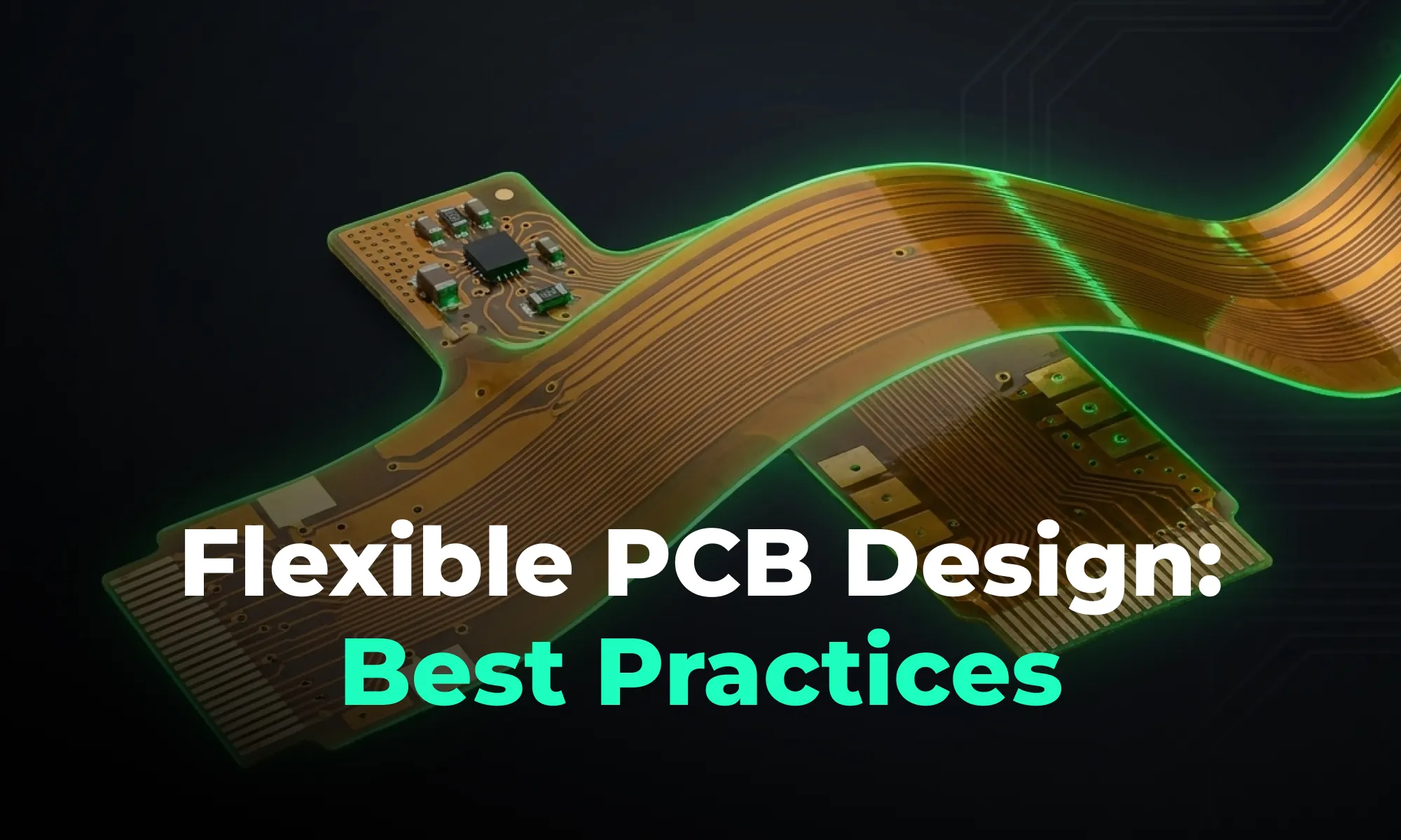
A guide to flexible PCB design, covering materials, stackups, bend radius, and layout best practices for wearables, medical devices, and other compact electronics.

A beginner-friendly guide to reading PCB schematics, covering common symbols, nets, and how to follow signal flow through a circuit diagram.

An overview of collaborative PCB design, showing how cloud-native tools, real-time editing, and shared libraries are reshaping modern hardware team workflows.

A guide to managing PCB component libraries, covering symbols, footprints, and 3D models with best practices for standardizing parts across hardware teams.

An overview of PCB reverse engineering, explaining how engineers analyze boards, extract schematics, and use the process for legacy support, repair, and design analysis.
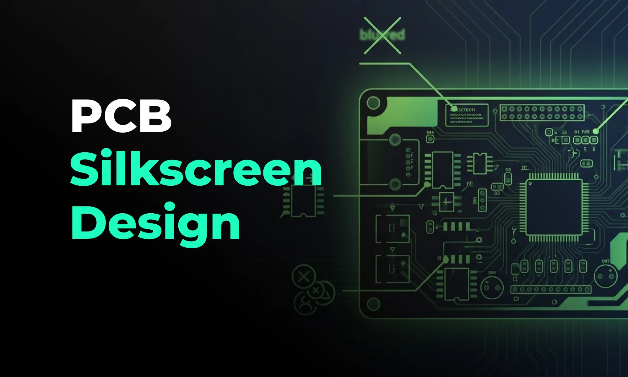
A practical guide to PCB silkscreen design, covering labeling best practices, common readability mistakes, and how clean silkscreens improve assembly and debugging.

An explainer on PCB version control, comparing hardware revision workflows to Git-style collaboration and showing how modern teams track design changes.
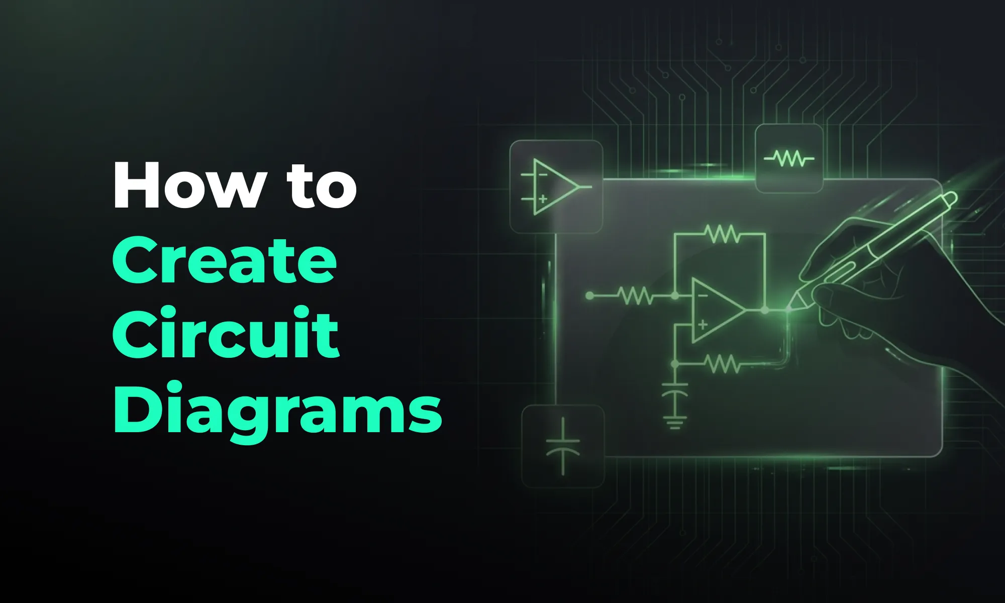
An introduction to schematic capture, explaining how engineers use symbols, nets, and connectivity to create circuit diagrams that drive PCB layout.
