September 21, 2023
Understanding the Fundamentals: MOSFET Basics for Beginners
Share

A MOSFET is a specific type of FET (Field-Effect Transistor) that utilizes an electric field to control the flow of current between its source and drain terminals. Unlike BJTs (Bipolar Junction Transistors), which are current-controlled devices, MOSFETs are voltage-controlled, offering advantages in terms of power consumption and switching speed.
They're used in a wide range of applications due to their unique properties, such as high input impedance and fast switching capabilities. Some of the primary uses of MOSFETs include:
A MOSFET typically has three primary pins, though some specialized versions can have additional pins. Here are the three standard pins:

The operation and behavior of the MOSFET depend on whether it's an N-channel (NMOS) or P-channel (PMOS) type, as well as whether it's enhancement-mode or depletion-mode. When looking at the physical package of the MOSFET, it's important to refer to the datasheet or use a multimeter to identify each pin, as the pin configuration can vary depending on the manufacturer and the package style (e.g., TO-220, SOIC, etc.).
Additionally, many MOSFETs have a fourth component, the Body or Substrate, which is often internally connected to the source in discrete MOSFETs. This connection forms what is called the "body diode" or "substrate diode", which can conduct in the reverse direction if biased appropriately.
Always refer to the datasheet of the specific MOSFET you are using for accurate pinout information and specifications.
A MOSFET can function both as a switch and as an amplifier, depending on how it is configured in a circuit.
A JFET is similar to a MOSFET but lacks the insulating layer between the gate and channel. They are generally used in analog signal applications but are less popular than a FET due to higher input capacitance and lower transconductance.
BJTs are current-controlled devices and are generally faster than MOSFETs. However, a BJT consumes more power and is less input-impedance-friendly compared to a FET.
The channel in a MOSFET is made of doped semiconductor material. Doping refers to the introduction of impurities into the semiconductor to increase its conductivity. The term "depletion" refers to the region near the junction where mobile charge carriers are depleted, affecting the MOSFET's electrical characteristics.
Understanding the fundamentals of a MOSFET, including key MOSFET parameters like Vgs and Vd, as well as the differences between NMOS, PMOS, and other types of transistors such as BJTs and JFETs, is crucial for anyone venturing into the field of electrical engineering. MOSFETs' low power consumption, high input impedance, and versatility make them indispensable in modern electronics.
By grasping these MOSFET basics, you'll be well-equipped to delve deeper into the intricacies of MOSFET semiconductor devices and their applications in various circuits.


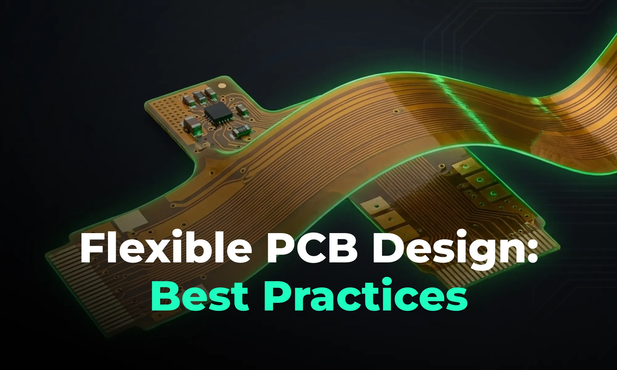
A guide to flexible PCB design, covering materials, stackups, bend radius, and layout best practices for wearables, medical devices, and other compact electronics.

A beginner-friendly guide to reading PCB schematics, covering common symbols, nets, and how to follow signal flow through a circuit diagram.

An overview of collaborative PCB design, showing how cloud-native tools, real-time editing, and shared libraries are reshaping modern hardware team workflows.

A guide to managing PCB component libraries, covering symbols, footprints, and 3D models with best practices for standardizing parts across hardware teams.

An overview of PCB reverse engineering, explaining how engineers analyze boards, extract schematics, and use the process for legacy support, repair, and design analysis.
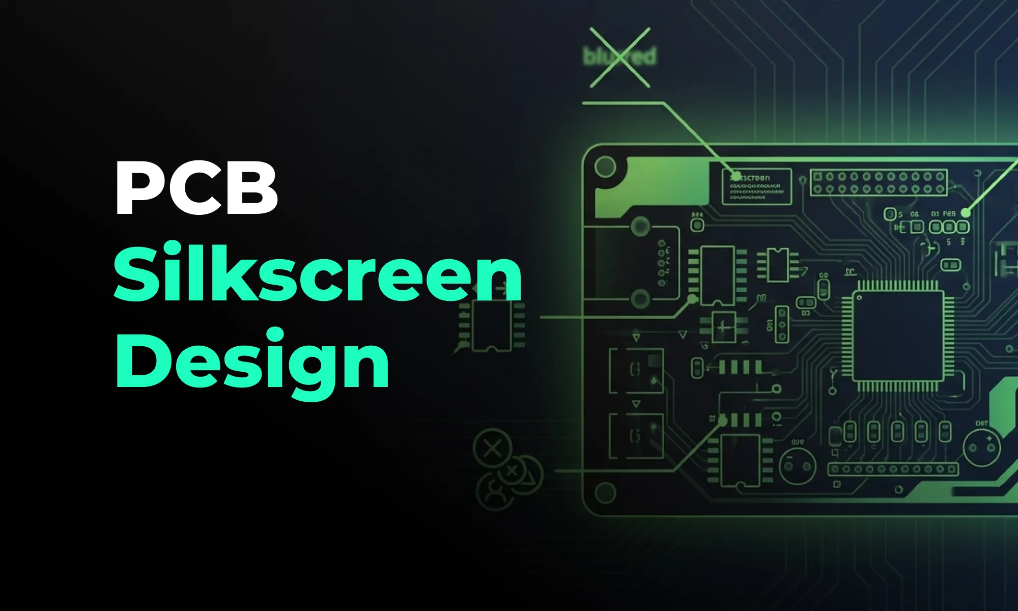
A practical guide to PCB silkscreen design, covering labeling best practices, common readability mistakes, and how clean silkscreens improve assembly and debugging.

An explainer on PCB version control, comparing hardware revision workflows to Git-style collaboration and showing how modern teams track design changes.
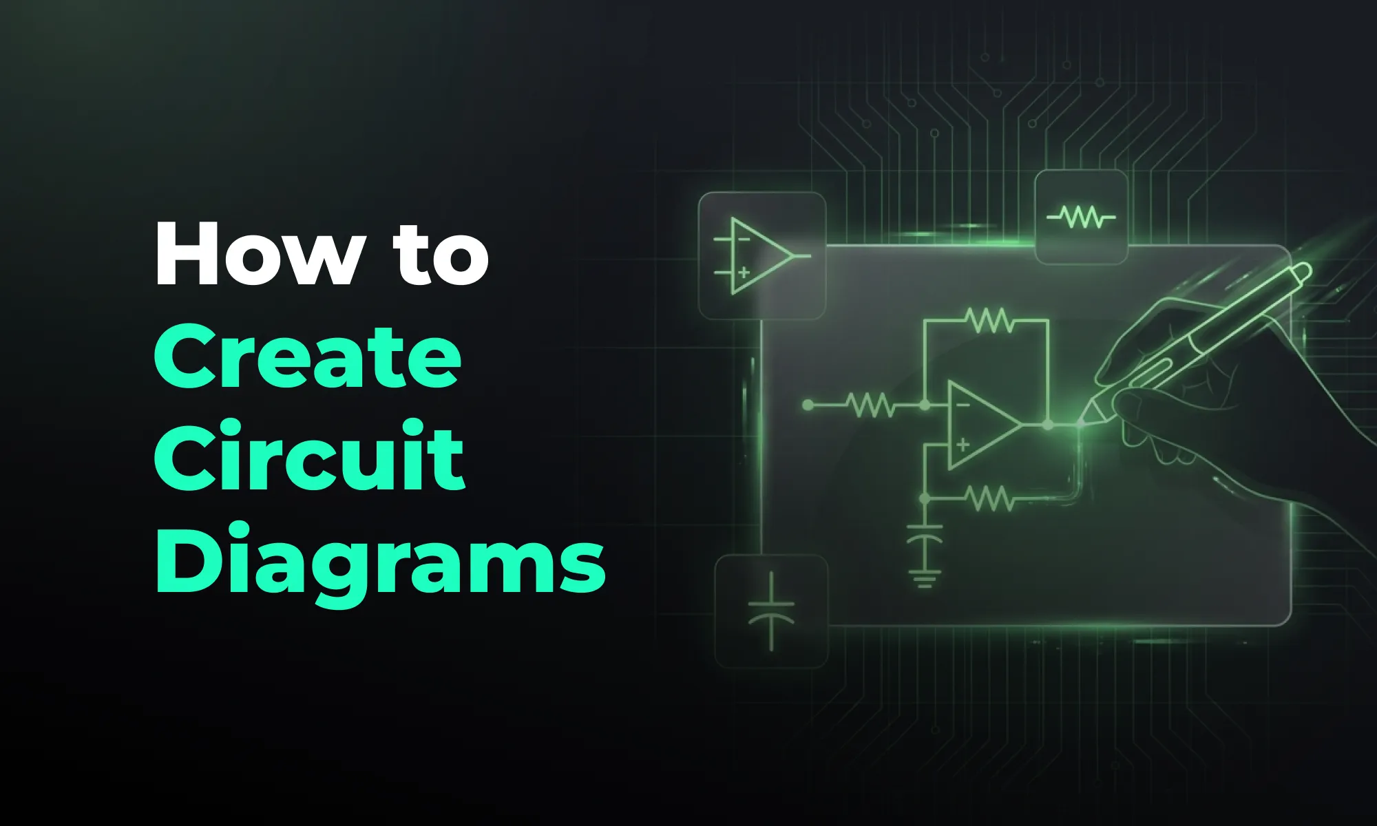
An introduction to schematic capture, explaining how engineers use symbols, nets, and connectivity to create circuit diagrams that drive PCB layout.
