June 9, 2023
Schematic Diagrams In Electronics
Share
BuildWithFlux


Every time a new electrical circuit board design comes to life, it all begins with an idea. This idea is then carefully planned and defined, using a combination of words, symbols, lines, and diagrams, in a detailed specification. While anyone can bring an idea this far, the next crucial step requires a solid grasp of electronic schematics.
Think of schematics as the bridge that connects the conceptual electrical design to the creation of a printed circuit board assembly (PCBA). It's the missing link that brings the idea to life and turns it into a tangible reality.
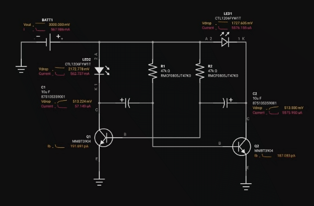
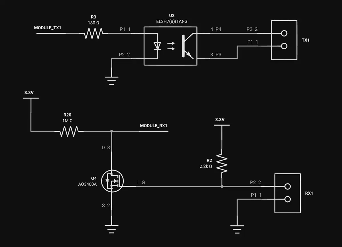
A schematic diagram, or schematic drawing, is a fundamental two-dimensional circuit representation showing the functionality and connectivity between different electrical components. It's composed of electronic symbols, wiring diagrams, designators, net names, and netlist. A PCB designer needs to get familiarized with the schematic symbols that represent the components on a schematic diagram. These symbols serve as a universal language understood by engineers, technicians, and electricians across different industries. They provide a concise and standardized way of communicating circuit designs.
A schematic block diagram also referred to as a block diagram or a functional diagram, is a simplified representation of a system or a process using blocks to represent its various components or stages. It provides an overview of the system's structure and the interconnections between its major functional units or subsystems.
In a schematic block diagram, each block represents a specific component, module, or function within the system. The blocks are typically labeled with descriptive text to indicate their purpose or functionality. The interconnections between the blocks are represented by lines or arrows, indicating the flow of signals, information, or energy between the different components or stages.
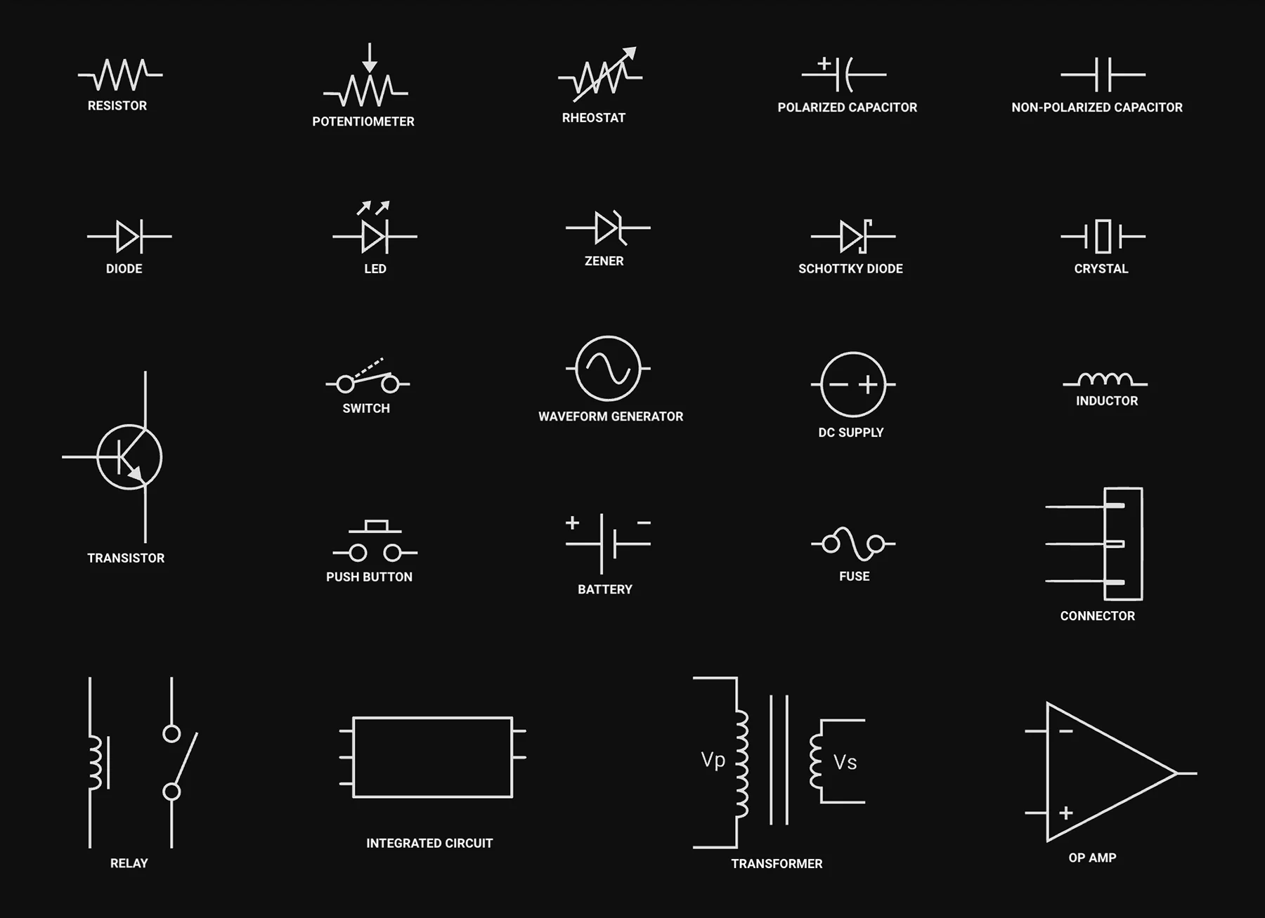
Schematic symbols are typically designed to visually represent the physical characteristics, electrical properties, and functionality of components. They are usually simple, abstract, and intuitive, allowing quick recognition and identification.
For example, a resistor in a circuit diagram is represented by a zigzag line, which indicates its function of restricting current flow. A capacitor is depicted by two parallel lines separated by a gap, representing its ability to store electrical energy. Symbols exist for diodes, transistors, switches, connectors, IC (integrated circuits), and many other components used in electrical circuits and electronic circuits.
Each component in a schematic diagram is assigned a component designator or reference designator (REFDES) to indicate its specific function within the circuit. It is a letter or combination of letters used to identify individual components within a circuit diagram uniquely. The designators serve as labels or identifiers for the components and are typically placed next to the corresponding symbols in the circuit diagram. It is important to follow a consistent and well-defined designator system within a circuit diagram to ensure clear communication and easy referencing of components.
Reference designators play a crucial role in the connection to the bill of materials (BOM). The BOM contains the part number for each component in your PCBA design and specifies where each part should be installed, based on its reference designator (REFDES).
Here are industry-standard formats for reference designators including a letter, indicating the type of component, followed by a number. For example R1, R2, R3.. etc
IEC 60617 and ANSI standard Y32 are two widely recognized and used standards for schematic diagram symbols and graphical representations in electrical and electronic circuit diagrams. These standards provide guidelines for the consistent depiction of components, connections, and other elements in circuit diagrams, ensuring clear communication and interoperability.
Both standards cover a wide range of components, including passive elements (resistors, capacitors, inductors), active devices (transistors, diodes), power sources, switches, connectors, logic gates, and more. They are periodically updated to incorporate new symbols, reflect technological advancements, and address industry needs.
The schematic diagram should provide this additional information to ensure that appropriate components are selected. The resistor should have its resistance value expressed in ohms (Ω). The battery should state its potential difference (voltage) expressed in volts. Other components are described in different terms. For example, capacitors differ by their capacitance value expressed in farads (F), and inductors are differentiated by their inductance value expressed in Henrys (H).
Additional attributions can be given to the symbols like power ratings, values, tolerances, etc. This helps us in identifying the correct components for the circuit. Here are common attributes of a component are:
A schematic diagram, or schematic drawing, is a fundamental two-dimensional circuit representation showing the functionality and connectivity between different electrical components. It's composed of electronic symbols, wiring diagrams, designators, net names, and netlist. A PCB designer needs to get familiarized with the schematic symbols that represent the components on a schematic diagram. These symbols serve as a universal language understood by engineers, technicians, and electricians across different industries. They provide a concise and standardized way of communicating circuit designs.
A schematic block diagram also referred to as a block diagram or a functional diagram, is a simplified representation of a system or a process using blocks to represent its various components or stages. It provides an overview of the system's structure and the interconnections between its major functional units or subsystems.
In a schematic block diagram, each block represents a specific component, module, or function within the system. The blocks are typically labeled with descriptive text to indicate their purpose or functionality. The interconnections between the blocks are represented by lines or arrows, indicating the flow of signals, information, or energy between the different components or stages.
Schematic symbols are typically designed to visually represent the physical characteristics, electrical properties, and functionality of components. They are usually simple, abstract, and intuitive, allowing quick recognition and identification.
For example, a resistor in a circuit diagram is represented by a zigzag line, which indicates its function of restricting current flow. A capacitor is depicted by two parallel lines separated by a gap, representing its ability to store electrical energy. Symbols exist for diodes, transistors, switches, connectors, IC (integrated circuits), and many other components used in electrical circuits and electronic circuits.
Each component in a schematic diagram is assigned a component designator or reference designator (REFDES) to indicate its specific function within the circuit. It is a letter or combination of letters used to identify individual components within a circuit diagram uniquely. The designators serve as labels or identifiers for the components and are typically placed next to the corresponding symbols in the circuit diagram. It is important to follow a consistent and well-defined designator system within a circuit diagram to ensure clear communication and easy referencing of components.
Reference designators play a crucial role in the connection to the bill of materials (BOM). The BOM contains the part number for each component in your PCBA design and specifies where each part should be installed, based on its reference designator (REFDES).
Here are industry-standard formats for reference designators including a letter, indicating the type of component, followed by a number. For example R1, R2, R3.. etc
IEC 60617 and ANSI standard Y32 are two widely recognized and used standards for schematic diagram symbols and graphical representations in electrical and electronic circuit diagrams. These standards provide guidelines for the consistent depiction of components, connections, and other elements in circuit diagrams, ensuring clear communication and interoperability.
Both standards cover a wide range of components, including passive elements (resistors, capacitors, inductors), active devices (transistors, diodes), power sources, switches, connectors, logic gates, and more. They are periodically updated to incorporate new symbols, reflect technological advancements, and address industry needs.
The schematic diagram should provide this additional information to ensure that appropriate components are selected. The resistor should have its resistance value expressed in ohms (Ω). The battery should state its potential difference (voltage) expressed in volts. Other components are described in different terms. For example, capacitors differ by their capacitance value expressed in farads (F), and inductors are differentiated by their inductance value expressed in Henrys (H).
Additional attributions can be given to the symbols like power ratings, values, tolerances, etc. This helps us in identifying the correct components for the circuit. Here are common attributes of a component are:


Arduino and Raspberry Pi are two of the most popular single-board computers used by electrical engineers for various projects. Both have their own strengths and weaknesses, and choosing between the two depends on the specific requirements of a project.

The Raspberry Pi Zero 2 W is a small and powerful computer with impressive performance for its size and price. With a quad-core processor, 512MB of RAM, built-in wireless connectivity, and a USB On-The-Go port, it's suitable for many projects, including home automation, media centers, and robotics.

ESP32 microcontrollers are affordable, low-power SoCs with integrated Wi-Fi and Bluetooth. Offering dual-core processing, ample memory, and versatility, they excel in IoT, wearables, and smart home applications. The ESP32's continuous evolution promises exciting possibilities ahead.
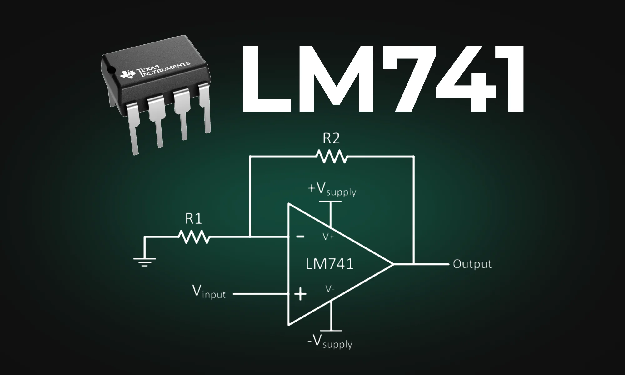
The blog post provides an in-depth look at the LM741 pinout diagram, explaining the functions of each pin, including inverting and non-inverting inputs, and comparing the LM741 to the LM324. It also covers various applications of the LM741 as an amplifier and a comparator.

The Arduino Pro Micro is a compact microcontroller within the Arduino ecosystem, based on the ATmega32U4. It's ideal for small applications, offering 20 digital I/O pins, built-in USB support, and easy programming. While having some limitations, its flexibility makes it popular for wearables, robotics, and DIY projects.

Streamline PCB development with NextPCB templates in Flux, featuring pre-set constraints, AI-assisted layouts, and seamless manufacturing transitions.
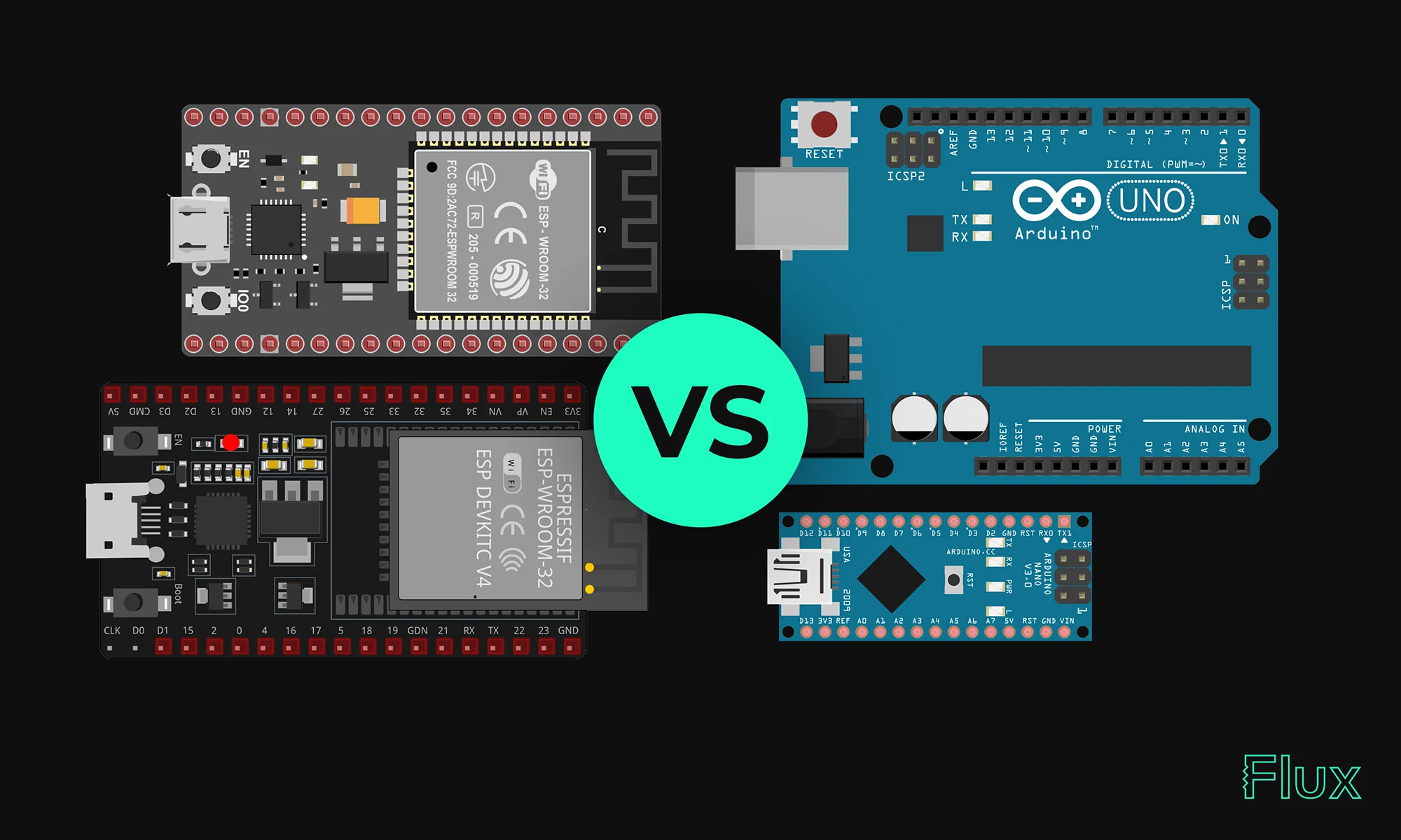
Our 2023 guide compares ESP32 and Arduino, two essential microcontrollers in IoT. ESP32 offers advanced features like Wi-Fi, while Arduino excels in ease of use and community support. Choose based on your project's complexity and needs.

Dive into the world of DIY Arduino projects, learning everything from choosing the right board to creating advanced home automation systems.


Effortlessly calculate parallel and series resistor values with our accurate, user-friendly tool designed to optimize circuit performance and streamline electrical design processes.
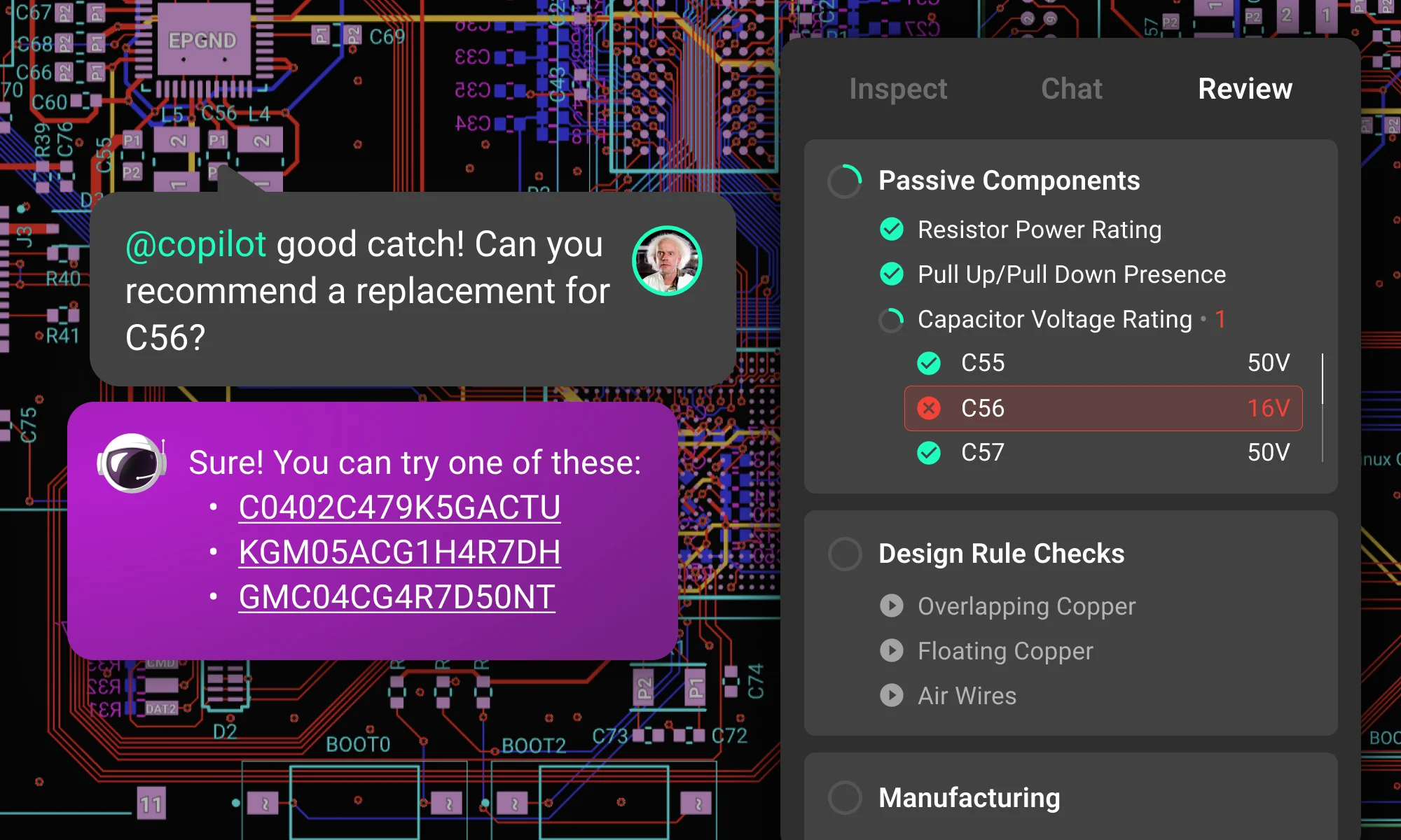
Creating a manufacturable, error-free PCB is never simple. Every engineer knows that missed details lead to production delays, costly revisions, and project setbacks. But what if you could have the power of a seasoned review team guiding you, 24/7?


Before you start this exciting journey, it's essential to equip yourself with the right knowledge, tools, and preparations. This article offers practical insights and suggestions to help you lay a strong foundation for your PCB design projects.

Think you're familiar with the push button and its symbol? Prepare to be surprised! Join us in our latest blog post where we unravel the intricate science behind every press, click, and circuit, revealing the complexities hidden in the simplicity of a push button switch.