November 10, 2023
Why Atmega328p is Still a Top Choice for Microcontroller Projects in 2023
Share
At the core of many electronic projects lies the ATmega328p, an 8-bit microcontroller belonging to Atmel's AVR series running off of a Reduced Instruction Set Computer (RISC) architecture. RISC architecture is advantageous due to its simplicity, which results in faster execution, improved compiler optimization, and better support for parallelism.
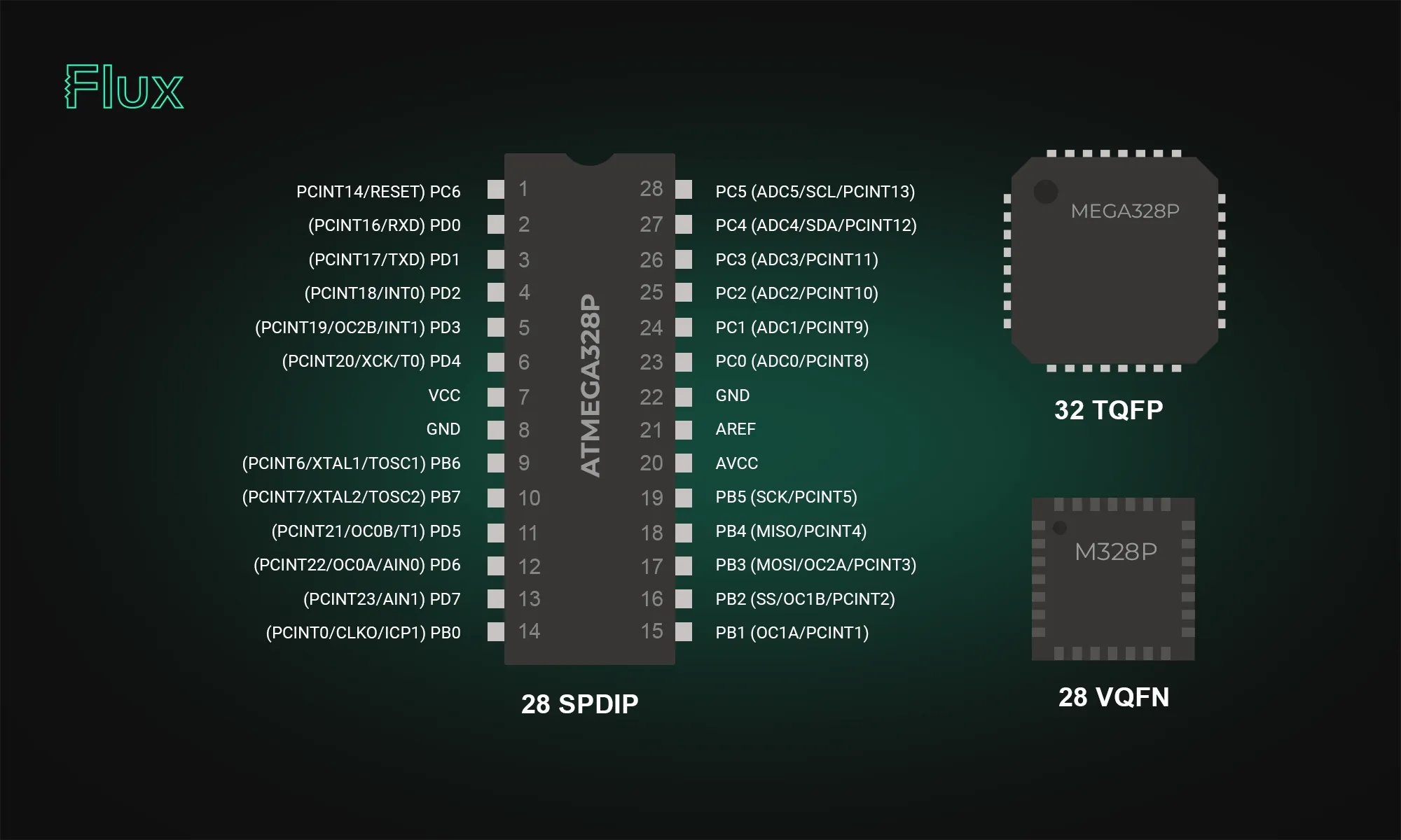
The ATmega328p is equipped with 32KB of ISP (In-System Programmable) flash memory, 1KB of EEPROM (Electrically Erasable Programmable Read-Only Memory), and 2KB of SRAM (Static Random-Access Memory).
Embedded systems often require the ability to store data persistently. The ATmega328p addresses this need with its onboard EEPROM. This non-volatile storage space is crucial for storing data that needs to persist across power cycles.
Developers can utilize the EEPROM for storing configuration parameters, calibration data, or any other critical information that requires retention.
With 32 pins, the large number of digital and analog I/O pins is a key strength of the Atemga328p. The device boasts 23 general-purpose I/O (GPIO) lines, including analog inputs for sensor integrations. With a total of 6 analog input pins, developers can seamlessly interface with various sensors, converting real-world analog signals into digital data for processing.
There are two VCC pins (pin 4 and pin 6) and one AVCC pin (pin 18) for voltage supply, three GND pins (pin 3, pin 5, and pin 21) for grounding, and additional pins for 22pF capacitors, vital for stabilizing the 16MHz crystal oscillator.
The ATmega328p excels in managing inputs and outputs with three bi-directional GPIO ports, two 8-bit ports—PortB and PortD–and one 7-bit port–PortC. These ports serve as I/O interfaces, allowing users to control or read from external devices. Each I/O port pin may be configured as an output with symmetrical drive characteristics, or an input with or without pull-up resistors of 20 - 40 K ohms. Each bit in a Port corresponds to a specific pin, granting granular control over the connected peripherals. Understanding the DDR (Data Direction Register) is crucial for manipulating the ports. It determines whether each pin in a port operates as an input or output. For instance, setting a specific bit in DDRB to 1 configures the corresponding pin in PortB as an output.
Ensuring a stable 5V supply is vital for consistent performance, and the ATmega328p comes equipped with robust voltage regulation capabilities. The microcontroller operating voltage range is 1.8V to 5.5V, making it adaptable to various power supply configurations.
The ATmega328p offers several power-saving modes, allowing developers to tailor power consumption based on project requirements. These modes are particularly beneficial for energy-sensitive applications, extending battery life, or enabling solar-powered solutions.
Notable features of the ATmega328p include a plethora of options for serial communication (SPI, I2C, USART), two 8-bit Timer/Counters, one 16-bit Timer/Counter, and a 6-channel 10-bit A/D converter (ADC) enabling analog signal acquisition.
The atmega328p supports SPI, I2C, and USART, essential for communicating with other microcontrollers or modules.
A dedicated SPI interface enables high-speed, full-duplex communication. The following table outlines the key pins associated with SPI:
Integrating SPI-enabled devices, such as external flash memory or display modules, becomes seamless with the ATmega328p.
I2C support further extends the microcontroller's communication capabilities. The ATmega328p's I2C pins are:
This protocol is invaluable in projects requiring communication with multiple devices on the same bus.
USART enables serial communication and is crucial for interfacing with devices like GPS modules or Bluetooth modules. The USART pins on the ATmega328p are:
The ATmega328p provides flexibility in choosing between internal and external clock sources. This choice, such as opting for an external 16MHz crystal, significantly influences precision and power consumption.
Built-in timer counters enable the ATmega328p's time-sensitive capabilities. These timers provide accurate timing intervals and pulse-width modulation (PWM) functionality.
The ATmega328p’s 6-channel 10-bit Analog-to-Digital Converter (ADC) significantly enhances its capability to acquire and process analog signals. This ADC functionality is instrumental in translating real-world analog data, such as sensor inputs, into digital values that can be processed by the microcontroller.
This module is capable of translating analog voltages into a 10-bit number ranging from 0 to 1023, based on the inputted range of expected voltages (from 0 V to the voltage of the VCC). The microcontroller provides flexibility in choosing from six input sources, but only one channel can be converted at a time. The ADC module operates with a conversion speed of approximately 15,000 samples per second (15 ksps), ensuring swift and efficient signal processing.
The ATmega328 and ATmega328P are microcontrollers from the same family but have some differences:
The ATmega328P is not discontinued. While there was an indication on a distributor's website (Mouser) suggesting that the ATmega328P-MU variant is scheduled for obsolescence and will be discontinued by the manufacturer, this information should be interpreted with caution.
The Arduino Uno board, one of the most popular Arduino boards, uses the ATmega328p as its central processing unit. This integration has played a significant role in popularizing the ATmega328p, making it synonymous with user-friendly yet powerful microcontroller projects.
While Arduino offers easy access to the ATmega328’s capabilities, there are some applications that require utilizing the ATmega328p standalone, without the Arduino framework. Programming the ATmega328p standalone has a steeper learning curve, but provides a more granular and customized approach.


Learn about STM32 microcontrollers, popular series, USB OTG, SWD, UART, and development tools. Find the right STM32 MCU and kickstart your projects.
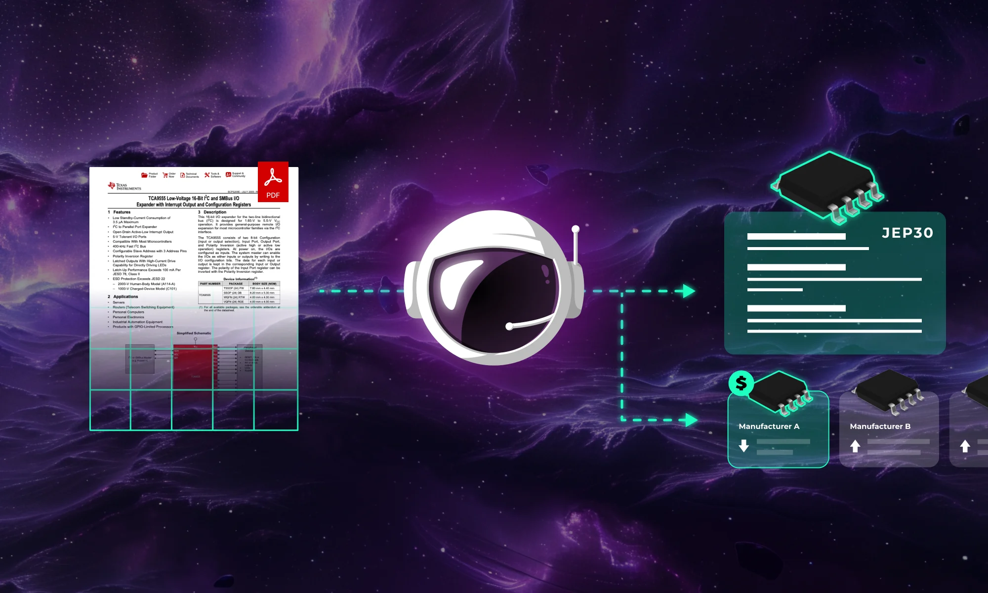
Discover how CAD Librarians can leverage Flux’s key capabilities—AI Part Imports, Component Updates, Live Pricing, and JEP30 Export—each tailored to meet the specific demands of maintaining PCB libraries.

Despite newer technologies like USB and Ethernet, RS232 remains widely used due to its simplicity and broad compatibility. It's crucial in industries, scientific instruments, networking gear, and legacy computers. This protocol's reliability makes it the go-to for many applications. In this blog, we'll explore why RS232 continues to be relevant in our tech-savvy world.
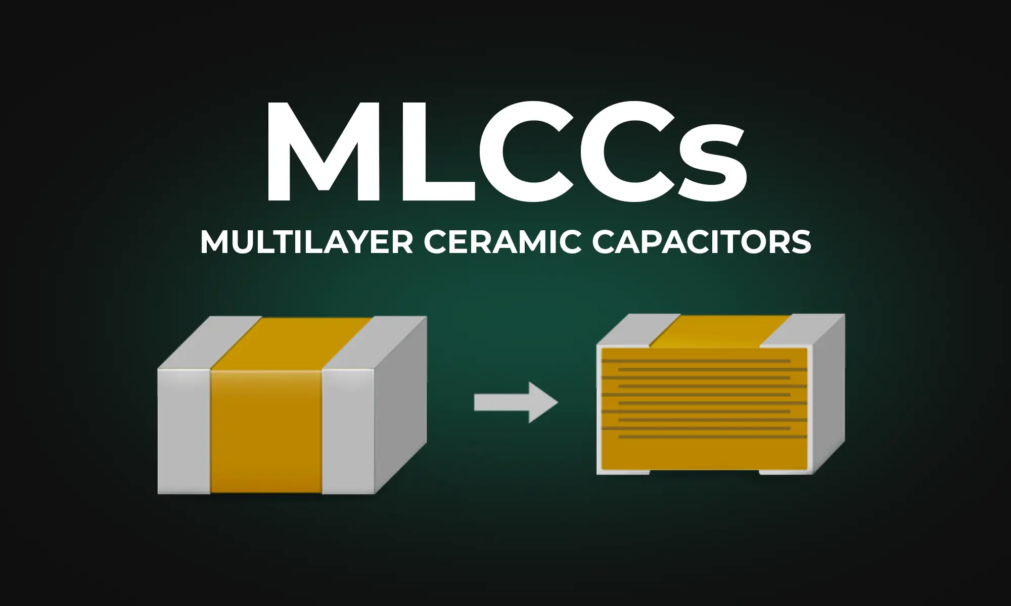
The blog post dives into the technical aspects of Multilayer Ceramic Capacitors (MLCCs), highlighting their importance in electronic circuits. It explains the construction of MLCCs, where layers of ceramic material and metal electrodes create a multilayered structure to store electrical energy.

The blog offers an in-depth look at Zener diodes, highlighting their crucial role in voltage regulation and stability in electronic circuits. It covers their basic principles, applications, and the challenges faced in their usage.

Looking for a comprehensive guide to ESP8266 pinout? Check out our article that covers everything you need to know about the ESP8266's pins, including digital, analog, and PWM pins. Perfect for beginners and experts alike, our guide will help you understand the ESP8266's pinout and how to use it in your projects.

Think you're familiar with the push button and its symbol? Prepare to be surprised! Join us in our latest blog post where we unravel the intricate science behind every press, click, and circuit, revealing the complexities hidden in the simplicity of a push button switch.

Oscillators are electronic circuits producing oscillating signals without an input. Types include sine, square, sawtooth, triangular, and pulse wave oscillators. Crystal oscillators use vibrating crystals for precise frequencies, crucial in clocks and radios. RF oscillators operate at radio frequencies, essential in broadcasting and telecoms.
