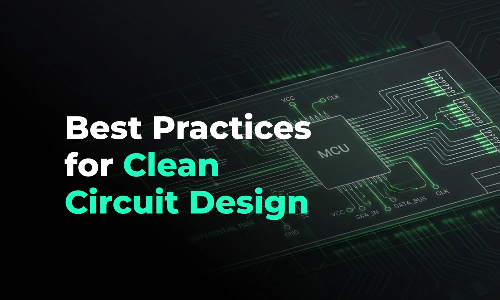
A printed circuit board starts with a schematic. Before any components are placed in a physical layout or any copper traces are routed, the schematic defines the electrical structure of the design. Schematic serves as a communication tool that engineers use to describe how a system functions.

If a schematic is drawn poorly, it leads to confusion, routing errors, and massive delays during the debugging phase. Successful PCB schematic design means prioritizing readability and organization. This guide covers the foundational rules and PCB schematics best practices required to create professional, maintainable, and error-free circuit diagrams.

Key Takeaways

  • Schematics are a language for circuit: A well-drawn schematic communicates intent clearly to other engineers, layout designers, and test technicians.
  • Directional flow matters: Standardizing signal flow from left to right, and power from top to bottom, makes troubleshooting significantly faster.
  • Net labels prevent clutter: Using local and global net labels instead of drawing long, crossing wires prevents the "spaghetti" effect.
  • Modern tools enhance teamwork: Cloud-native platforms like Flux eliminate isolated workflows, allowing multiple engineers to review and edit schematics simultaneously.

Why Good PCB Schematic Design Matters

In the rush to get to the physical board layout, beginners often throw their circuit schematics together haphazardly. While the software might still generate a valid netlist, ignoring PCB schematic best practices introduces severe long-term risks.

  • Readability: Electronics projects are rarely built by a single person. If you hand off your design to a colleague or a client, they need to understand the architecture immediately. A clean layout acts as its own documentation.
  • Debugging Efficiency: When a physical prototype fails on the test bench, technicians use the schematic to trace signals and find test points. If the schematic is an unreadable maze, debugging takes hours instead of minutes.
  • Collaboration Benefits: In complex designs, different engineers might design different sub-circuits (e.g., one designs the power supply, another the RF antenna). Organized, block-based schematics allow teams to merge their work without causing electrical conflicts.

How Engineers Organize Circuit Schematics

PCB schematic design relies on predictable, standardized organization. Just as you read a book in a specific direction, engineers expect to read a schematic following certain physical rules.

Signal Flow Direction

Always design your signal flow to move from left to right.

  • Place inputs (connectors, power jacks, sensors) on the left side of the sheet.
  • Place processing components (microcontrollers, op-amps) in the center.
  • Place outputs (displays, LEDs, motor drivers) on the right side.

For power circuits, use a top-to-bottom flow. Place positive voltage symbols (e.g., +5V, +3.3V) pointing upward at the top of the component, and place ground (GND) symbols pointing downward at the bottom.

Grouping Circuits

Do not dump all components onto a single, massive sheet. Break the design into logical functional blocks. Use drawing tools (like bounding boxes or dashed lines) to visually group the "Power Management" section separately from the "Memory Interface" section.

For advanced designs, utilize hierarchical schematics, where a top-level block symbol represents an entire sub-sheet of circuitry. In practice, this can be implemented as multi-sheet hierarchies, where each block lives on its own schematic page and is connected through defined ports or net labels. Some modern EDA tools, such as Flux, also support modular or reusable schematic blocks, allowing designers to encapsulate circuits as self-contained modules that can be reused across different projects while maintaining a consistent structure.

Labeling Conventions

Instead of drawing a continuous wire from a microcontroller pin all the way across the page to a sensor, use net labels. Assigning a name like I2C_SDA to a short wire stub automatically connects it to any other wire stub with the exact same name. This keeps clean circuit diagrams free of long, overlapping lines.

Best Practices for Schematic Symbols and Nets

The foundation of all PCB circuit diagrams rests on the proper use of lines (nets) and shapes.

Schematic Symbols

A schematic symbol is the logical representation of a physical component.

  • Always use standardized, verified schematic symbols.
  • Ensure that the pins on the symbol logically match the manufacturer's datasheet.
  • Organize the pins on the symbol by function, not by physical location. (For example, group all GND pins together at the bottom of the symbol, even if they are on opposite sides of the microchip).

Nets, Junctions, and Crossing Lines

Nets are the wires connecting your components. Understanding how nets intersect is one of the most important schematic-reading skills.

  • Junction (Connection): When two or more nets meet and there is a solid dot at the intersection, the wires are electrically connected. Junctions are commonly used where power or ground branches to multiple components, such as several ICs sharing the same 3.3V supply.
  • Crossing (No Connection): When two nets cross without a dot, they are not electrically connected. The lines simply pass over each other on the drawing. This is common in larger schematics where signals must cross paths without creating unintended connections.

Crucial Rule: Never create a four-way junction (a "+" intersection). A four-way crossing can be ambiguous because it may be unclear whether the wires are connected or merely crossing. Instead, break the connection into two separate three-way "T" junctions, each marked with a junction dot where a connection is intended. This makes the electrical intent clear and prevents wiring mistakes.

Best Practices for Schematic Symbols, Nets, and Layout

Category Best Practice
Signal Flow Direction Design signals left-to-right and power top-to-bottom
Inputs Placement Place connectors, sensors, and inputs on the left
Processing Blocks Keep MCUs, op-amps, and logic ICs in the center
Outputs Placement Place LEDs, displays, and drivers on the right
Power Rails Route positive rails at top and ground at bottom
Grouping Circuits Divide schematic into functional blocks
Hierarchical Design Use multi-sheet or modular schematic blocks
Net Labels Use named nets instead of long wires
Schematic Symbols Use standardized symbols aligned with datasheets
Pin Organization Group pins by function, not physical package layout
Net Connections (Junctions) Use a solid dot to indicate electrical connection
Net Crossings Crossing lines without dots are not connected
4-Way Junction Rule Never use "+" style junctions; use two T-junctions instead

How to Improve Schematic Readability

Adhering to strict schematic layout best practices ensures your work remains legible. Use the following checklist before finalizing your design:

Clean Schematic Checklist

  • Consistent Spacing: Leave adequate breathing room around components. Do not cram symbols together just to save page space.
  • Clear Labels: Rename default nets (like Net0012) to descriptive names (like 5V_MAIN or UART_TX).
  • Avoid Crossing Wires: Minimize the number of times lines intersect. Use net labels to bridge distant connections.
  • Align Components: Snap components and texts to the grid. Aligning resistors and capacitors neatly makes the circuit visually harmonious.
  • Add Text Notes: Use text boxes to leave notes for the layout designer (e.g., "Keep these traces short" or "Place near IC").

Common PCB Schematic Mistakes

Even experienced engineers occasionally fall into bad habits. Watch out for these frequent errors:

  • Messy Layouts (Spaghetti Wiring): Drawing every single connection as a physical line creates a tangled web that is impossible to decode and prone to accidental crossed wires.
  • Poor Labeling: Failing to add reference designators (e.g., leaving a part labeled as R? instead of R14) breaks the link between the schematic and the physical PCB layout.
  • Inconsistent Symbols: Mixing US (ANSI) and European (IEC) symbol standards on the same page, or drawing custom symbols that don't clearly indicate inputs versus outputs.
  • Hidden Power Pins: Some legacy software hides power and ground pins on logic gates by default. Always ensure power pins are visible and explicitly connected to the correct voltage rails.

How Modern PCB Tools Improve Schematic Design

Historically, schematic organization was a solitary task tied to legacy desktop software. If an engineer wanted a peer review, they had to export a PDF and wait for feedback via email.

Modern platforms like Flux have reimagined this workflow by bringing PCB schematic design into the browser. Flux is inherently collaborative, offering a "multiplayer" environment where hardware engineers, layout designers, and firmware developers can view, comment on, and edit the same schematic simultaneously.

Because Flux acts as a unified platform, schematic symbols are deeply integrated with their physical footprints and 3D models. The software also utilizes an AI Copilot that can help beginners understand complex circuit blocks or automatically wire standard components. Try Flux to explore interactive schematics and use AI-powered Copilot to explain complex circuit blocks.

FAQs

What is PCB schematic design?
It is the process of drawing a logical, 2D representation of an electronic circuit using standardized symbols and wiring to show exactly how components connect electrically.
How should signal flow be organized in a schematic?
The standard engineering practice is to route signal flow from left (inputs) to right (outputs), and power flow from top (positive voltage) to bottom (ground).
What is a net label?
A net label is a text name assigned to a wire. It creates an invisible electrical connection to any other wire on the schematic sharing the exact same name, helping to reduce visual clutter.
Why should I avoid 4-way wire junctions?
A 4-way crossing (like a "+" sign) makes it visually ambiguous whether the wires are electrically connected or just passing over each other. Using two staggered "T" junctions removes all doubt.
What is the difference between a schematic and a PCB layout?
A schematic illustrates the logical electrical connections of a circuit. The PCB layout dictates the physical placement of those components and the routing of copper traces on the actual board.
Profile avatar of the blog author

Yaneev Hacohen

Yaneev Cohen is an electrical engineer concentrating in analog circuitry and medical devices. He has a Master's and Bachelor's in Electrical Engineering and has previously worked for Cadence and Synopsys's technical content departments.

Go 10x faster from idea to PCB
Work with Flux like an engineering intern—automating the grunt work, learning your standards, explaining its decisions, and checking in for feedback at key moments.
Illustration of sub-layout. Several groups of parts and traces hover above a layout.
Design PCBs with AI
Introducing a new way to work: Give Flux a job and it plans, explains, and executes workflows inside a full browser-based eCAD you can edit anytime.
Screenshot of the Flux app showing a PCB in 3D mode with collaborative cursors, a comment thread pinned on the canvas, and live pricing and availability for a part on the board.

Related Content

Component Selection in PCB Design: How Engineers Choose the Right Parts

Component Selection in PCB Design: How Engineers Choose the Right Parts

A guide to PCB component selection, covering electrical specs, footprints, thermal performance, sourcing, and best practices for picking parts that ship reliably.

Profile avatar of Yaneev Hacohen
Yaneev Hacohen
|June 15, 2026
PCB Design Reviews: Best Practices for Catching Errors Early

PCB Design Reviews: Best Practices for Catching Errors Early

A guide to PCB design reviews, covering schematic, layout, and DFM checks engineers use to catch errors early and ship more reliable boards.

Profile avatar of Yaneev Hacohen
Yaneev Hacohen
|June 15, 2026
How to Create and Manage PCB Footprint Libraries

How to Create and Manage PCB Footprint Libraries

A guide to creating and managing PCB footprint libraries, covering IPC standards, pad sizing, validation workflows, and best practices for reliable land patterns.

Profile avatar of Yaneev Hacohen
Yaneev Hacohen
|June 15, 2026
Flexible PCB Design Guide: Materials, Layout, and Applications

Flexible PCB Design Guide: Materials, Layout, and Applications

A guide to flexible PCB design, covering materials, stackups, bend radius, and layout best practices for wearables, medical devices, and other compact electronics.

Profile avatar of Yaneev Hacohen
Yaneev Hacohen
|June 8, 2026
How to Read PCB Schematics: A Beginner-Friendly Guide

How to Read PCB Schematics: A Beginner-Friendly Guide

A beginner-friendly guide to reading PCB schematics, covering common symbols, nets, and how to follow signal flow through a circuit diagram.

Profile avatar of Yaneev Hacohen
Yaneev Hacohen
|June 8, 2026
Collaborative PCB Design: Why Hardware Teams Are Moving to the Cloud

Collaborative PCB Design: Why Hardware Teams Are Moving to the Cloud

An overview of collaborative PCB design, showing how cloud-native tools, real-time editing, and shared libraries are reshaping modern hardware team workflows.

Profile avatar of Yaneev Hacohen
Yaneev Hacohen
|June 5, 2026
PCB Component Libraries: Best Practices for Managing Parts

PCB Component Libraries: Best Practices for Managing Parts

A guide to managing PCB component libraries, covering symbols, footprints, and 3D models with best practices for standardizing parts across hardware teams.

Profile avatar of Yaneev Hacohen
Yaneev Hacohen
|June 5, 2026
PCB Reverse Engineering: How It Works and When to Use It

PCB Reverse Engineering: How It Works and When to Use It

An overview of PCB reverse engineering, explaining how engineers analyze boards, extract schematics, and use the process for legacy support, repair, and design analysis.

Profile avatar of Yaneev Hacohen
Yaneev Hacohen
|June 5, 2026