June 15, 2026
PCB Design Reviews: Best Practices for Catching Errors Early
Share
A PCB design review is a structured quality gate where a board's schematic, layout, and manufacturing files (Gerbers or ODB++) are evaluated against electrical, mechanical, and functional requirements. It is a formal milestone in hardware development. The PCB design review passes the design only after rigorous verification, clearing the path for prototyping or volume fabrication.
PCB designs commonly undergo multiple respins as a result of signal integrity (SI), power integrity (PI), and electromagnetic interference (EMI) violations, with an average respin costing nearly $28,000. A realistic respin cost includes new bare boards, reassembly, expedited component handling, bench time, engineering debug, revised documentation, procurement friction, and the schedule cost of a blocked milestone.
Rather than eating the cost of these cascading delays, a formal PCB design review eliminates most of those line items before you have to sink money in for a respin.
To systematically catch the exact errors that drive these exorbitant costs, engineering teams evaluate the board against three specific categories of project risk:
Breaking the review into phased stages lets teams isolate different classes of errors.
Schematic Review focuses entirely on verifying circuit logic before any physical layout begins. Engineers validate component selection, net connectivity, power sequencing, and interface logic.
Layout Review evaluates the physical realization of that schematic. This phase covers component placement, routing topologies, thermal management, and stackup definition.
DFM (Design for Manufacturability) Review checks the layout against fabrication process constraints. IPC-2221C is the primary reference for generic PCB spacing and clearance rules. IPC-6012F is the current revision of the rigid board qualification standard. Your DFM review should call out which revision and class your fabricator is building to.
Use the following checklist as the minimum bar before design sign-off.
Even with automated software checks, certain layout mistakes consistently slip past designers. These oversights force expensive board revisions.
One persistent issue involves basic schematic connectivity. Unconnected or floating logic nets frequently escape initial routing checks and produce unpredictable behavior or complete functional failure. Footprint mismatches are equally common. For example, selecting an 0805 footprint for a 0603 physical part will lead to assembly failure and an immediate board revision.
Beyond electrical logic and physical part fit, you have to account for thermodynamics. Failing to plan for heat distribution during assembly introduces another layer of failure points. In practice, thermal imbalance causes reflow defects that are expensive to diagnose. Take a standard two-terminal component, for instance. Think about when a surface-mount pad connects directly to a heavy copper ground pour. If you forget a thermal relief, that solid plane acts like a massive heatsink. Such a mistake creates differential heating during the reflow process. Unsurprisingly, the pad tied to the plane stays much cooler than the opposite pad. As a result, the solder paste melts at significantly different rates.
Another common issue is signal integrity. More specifically, traces crossing split ground planes are an example. A high-speed signal needs a solid, continuous return path. When you route a trace over a gap in the reference plane, the return current has to detour. Such a detour causes an impedance mismatch. It radiates electromagnetic noise that will quickly fail EMC compliance testing.
| Defect Type | Description | Common Root Cause | Prevention Strategy |
|---|---|---|---|
| Tombstoning | Component stands on one end during reflow | Missing thermal relief on ground plane connections | Use symmetrical pads and appropriate thermal reliefs |
| Impedance Mismatch | Signal reflection causing data corruption | Traces crossing split reference planes | Route high-speed signals over solid, continuous ground planes |
| Floating Nets | Unpredictable logic states | Missing pull-up or pull-down resistors | Run comprehensive ERC and manual schematic checks |
| Footprint Mismatch | Assembly failure at placement | Wrong land pattern assigned in schematic library | Audit every footprint against the physical component datasheet |
Legacy review workflows rely on PDF plots or static design file exports, creating version control problems and communication bottlenecks. Resolving a single impedance issue can require a dozen email exchanges and marked-up screenshots before the designer can implement the fix.
Modern platforms like Flux shift teams from asynchronous file-based reviews to synchronous, AI-assisted validation. Flux provides:
Conducting a rigorous PCB design review doesn't have to mean endless PDF markups and disjointed email threads. To stop respins and keep your engineering teams aligned, try shifting your next hardware project to a modern collaborative environment. Flux's cloud-native architecture and AI-assisted validation tools make your PCB design review process faster, more accurate, and seamlessly integrated into your workflow.


A guide to PCB component selection, covering electrical specs, footprints, thermal performance, sourcing, and best practices for picking parts that ship reliably.
A guide to creating and managing PCB footprint libraries, covering IPC standards, pad sizing, validation workflows, and best practices for reliable land patterns.

A guide to PCB schematic best practices, covering organization, symbols, labeling, and readability tips for clean, maintainable circuit diagrams.
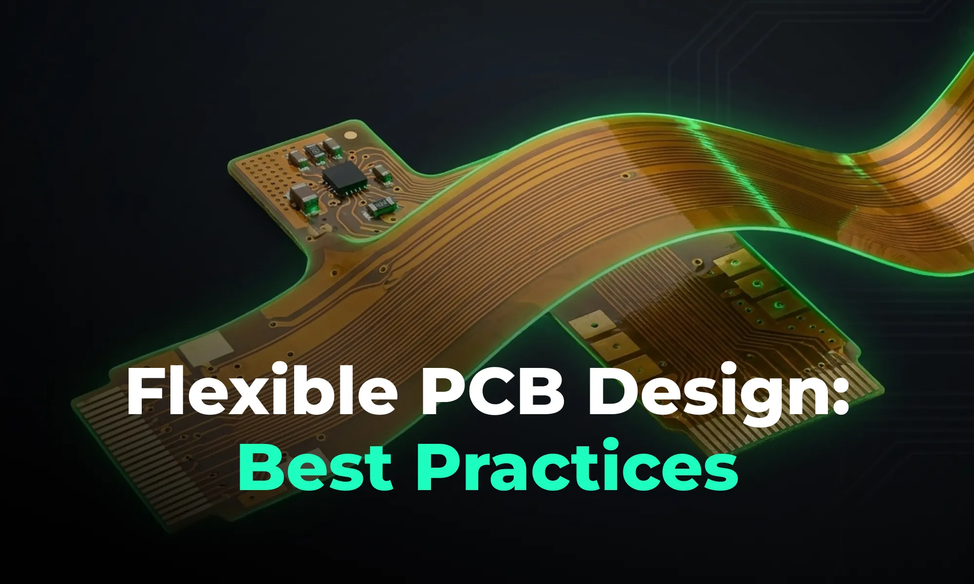
A guide to flexible PCB design, covering materials, stackups, bend radius, and layout best practices for wearables, medical devices, and other compact electronics.

A beginner-friendly guide to reading PCB schematics, covering common symbols, nets, and how to follow signal flow through a circuit diagram.

An overview of collaborative PCB design, showing how cloud-native tools, real-time editing, and shared libraries are reshaping modern hardware team workflows.

A guide to managing PCB component libraries, covering symbols, footprints, and 3D models with best practices for standardizing parts across hardware teams.

An overview of PCB reverse engineering, explaining how engineers analyze boards, extract schematics, and use the process for legacy support, repair, and design analysis.
