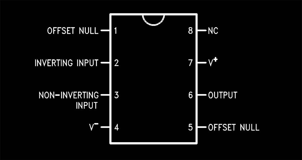
Before we dive into the pinout, let's clarify what an op amp is. An operational amplifier is a type of amplifier that takes a voltage input and provides an amplified voltage output. The degree of amplification is determined by the circuit configuration and the external components connected to the op amp. Now that we've set the stage, let's explore the pinout diagram of the LM741.
Understanding the pinout of an integrated circuit like the LM741 is crucial for proper application. A pinout diagram visually represents the functions of each terminal or pin on the IC. The LM741 typically comes in a Dual In-Line Package (DIP), but it is also available in SOIC (Small Outline Integrated Circuit) form. Whether you're looking at a DIP or SOIC package, the pinout remains nominally the same.

One of the first things to note on the LM741 pinout diagram are the inverting and non-inverting inputs. The inverting input is where the signal to be amplified is often fed when you're building an inverting amplifier circuit. Conversely, if you're designing a non-inverting amplifier, you'll use the non-inverting input.
The LM741 pinout also includes terminals for connecting the positive and negative voltage supplies (V+ and V-), essential for the amplifier's operation. Always consult the datasheet, often found on a .org or .com website, for the recommended voltage levels.
The offset null pins are used for offset voltage adjustment, critical in applications that require high precision. Offset is the dc voltage difference between the inverting and non-inverting inputs when the output is nominally zero volts.
The output pin provides the amplified voltage signal. Depending on the circuit configuration, the output can be in phase or out of phase with the input.
The LM324 is another popular opamp often considered alongside the LM741. While both are operational amplifiers, the LM324 has four opamps in a single IC, compared to the single opamp in an LM741. This allows for more flexibility in circuit design but complicates the pinout slightly.
You can use the LM741 in a variety of circuit applications, not just as an amplifier. For instance, it can function as a voltage comparator. A comparator takes two voltage inputs and outputs a voltage indicating which input is higher. In this role, the LM741 offers less precision than dedicated comparators but is often sufficient for simple tasks.
So there you have it, a comprehensive look at the LM741 pinout and its many applications, from its use as an amplifier to a comparator. This IC is not just a basic operational amplifier but a versatile component suitable for a wide range of voltage amplification and comparison tasks. Whether you’re a seasoned engineer or just starting out, the LM741 remains an essential tool in your electronics toolkit.
Remember, before plugging anything in, always refer to the pinout diagram and other resources from trusted .org or .com websites to ensure you're connecting everything correctly. Happy building!

A practical guide to calculating PCB trace resistance, covering the core formula, how geometry affects resistance, worked examples, and design tips to minimize voltage drop and heat.

A practical guide to diagnosing and fixing PCB failures, covering common symptoms, a step-by-step debugging workflow, essential tools (multimeter, oscilloscope, logic analyzer, thermal camera), a pre-power-up checklist, and the design mistakes that most often lead to broken boards.

A practical guide to PCB impedance control, covering why it matters for signal integrity, the four physical variables that shape trace impedance, and how to enforce impedance targets from stackup planning through routing and fabrication.

A practical guide to reducing EMI in PCB design through grounding, return path control, shielding, and layout best practices. Covers EMC compliance with CISPR 32 and FCC Part 15.

A step-by-step guide to designing accurate PCB footprints — covering pads, silkscreen, courtyards, IPC-7351 density levels, origin setup, and common mistakes to avoid.

A practical guide to PCB grounding techniques — ground planes, return paths, star grounding, and analog/digital partitioning — with best practices for reducing noise and improving signal stability.

A practical guide to designing multilayer PCB stackups for signal integrity, EMI control, and stable power delivery. Covers layer types, controlled impedance, common mistakes, and how modern tools simplify the process.

A look at how AI is reshaping PCB design by automating routing, placement, and signal integrity checks so engineers can focus on architecture and higher-level decisions.