September 1, 2023
Discovering PCB Manufacturing: Technologies That Shape the Industry
Share

The industry of PCB manufacturing has undergone significant transformations since its early days in the 20th century. Initially confined to single-sided circuit boards, technological advancements have enabled the development of more intricate double-sided and multilayer PCBs.
In today's technology-driven world, the importance of PCB manufacturing is monumental. These boards are essential for the functionality and reliability of a wide array of electronic systems, making their fabrication a cornerstone of industrial processes.
Single-sided PCBs feature only one layer of conductive material, typically copper, and are ideal for low-density designs. These types of circuit boards are prevalent in simple electronic devices like radios and sensors.
The fabrication involves applying a copper layer on one side of an insulating substrate. The unwanted copper is then etched away, leaving the desired circuit pattern. Soldering components onto the board follows this.
Double-sided PCBs have copper layers on both sides of the substrate, allowing for more complex circuits. These are commonly found in sophisticated devices like smartphones and automotive control systems.
The process includes applying copper layers on both sides of the substrate and connecting the layers using vias. Soldermask is then applied, followed by the HASL (Hot Air Solder Leveling) or ENIG (Electroless Nickel Immersion Gold) finishing process.
Multilayer PCBs consist of multiple conductive layers, separated by insulating material, and are used in highly complex systems like medical equipment and data servers.
The fabrication, or stackup, involves layering multiple sheets of copper and insulating material, which are then pressed together under heat and pressure. Circuit patterns are etched onto each layer, and vias are used to connect them.
The initial stage involves creating a detailed design of the circuit using CAD software, often incorporating DFM principles to ensure efficient manufacturing.
The substrate, usually made from materials like FR4 or Polyimide, is fabricated to provide mechanical support to the circuit board. This is followed by the stackup process, where multiple layers are combined.
Copper layers are applied to the substrate, and the circuit pattern is etched using chemical processes. The board then undergoes various finishing processes like applying soldermask and silkscreen, followed by HASL or ENIG surface finishing.
Emerging technologies like 3D printing and AI-driven optimization are set to redefine the PCB manufacturing sector.
The industry is increasingly focusing on sustainable materials and eco-friendly fabrication processes to mitigate environmental impact.
The demand for smaller, more efficient PCB boards presents both challenges, such as material limitations, and opportunities for innovation and technological breakthroughs.
Understanding the intricacies of PCB manufacturing, from the types of PCBs to the key stages in their fabrication, is crucial for anyone involved in the electronics or electrical engineering sectors. As technology continues to evolve, the PCB manufacturing industry is set for transformative developments that will significantly influence the future of electronics.


Flux's upgraded agent is more steerable, adaptive, and faster -- letting you change course mid-run, work in a single thread from idea to board, and ship hardware designs with less friction.
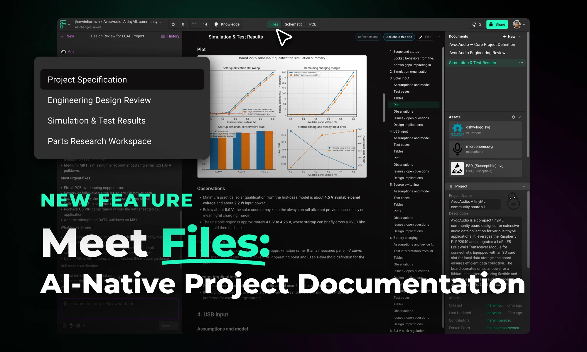
Flux Files centralizes your project docs, assets, and AI outputs in one tab so your team and AI always have the context they need.
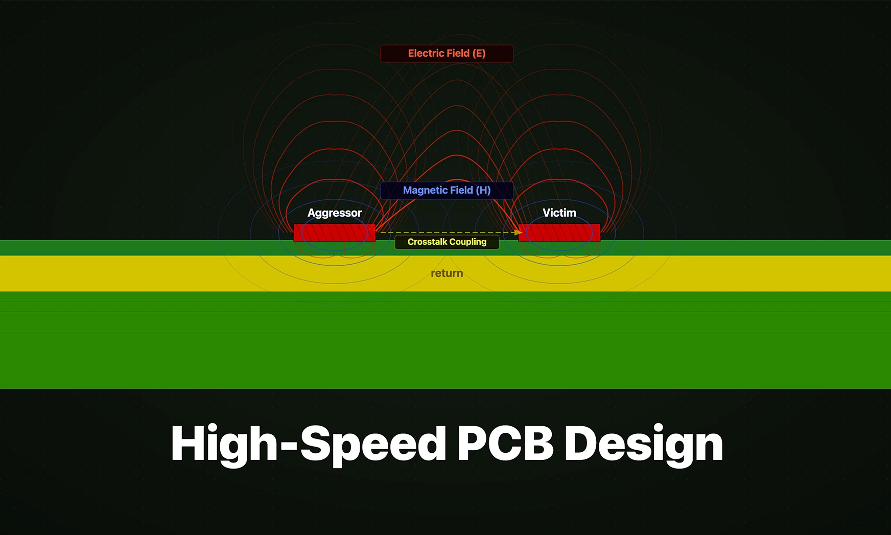
Whether you're migrating from popular EDA applications or starting fresh, mastering high speed PCB design has never been more intuitive. Flux enables teams to design, simulate, and route with real-time AI assistance, so you can spin your next high-speed board with total confidence.

This Spring 2026 updates make hardware design faster end-to-end with a more capable, self-correcting AI agent, improved AI auto-layout that needs less cleanup, sourcing-aware design with real-time pricing and availability, and templates to start from.

Today we’re excited to share that Flux has raised $37M in new funding led by 8VC, with participation from Bain Capital Ventures, Liquid 2 Ventures, and Outsiders Fund, alongside Lenny Rachitsky, John Lilly, and Tom Preston-Werner and many other world-class operators.

Flux's AI agent is now up to 10x faster and self-corrects in real time, delivering cleaner schematics with less waiting and fewer wasted credits.

This blog compares AI capabilities across Flux.ai, Altium, KiCad, and EasyEDA to answer engineers’ highest-intent questions about modern PCB design. It explains why Flux.ai currently delivers the strongest end-to-end AI workflow in the ECAD space.

Flux helps you design with live pricing and stock data, using AI to find in-stock parts and fast replacements before your BOM breaks.
