July 31, 2025

AI Auto-Layout Just Got Smarter

Flux Copilot astronaut points at a PCB with the text “Smarter AI Auto‑Layout” overlaid, highlighting the intelligence of Flux’s AI Auto‑Layout feature.

Today, we’re excited to share our Summer Update to Flux AI Auto‑Layout, a collection of improvements designed to make one‑click PCB routing more reliable, transparent, and adaptable to your real‑world workflows.

This update is a set of pragmatic steps toward our vision of Auto‑Layout as your trusted routing assistant. Here's what's improved:

  • Prioritize Nets with Net Types—add a ‘Net Type’ rule manually to your net properties or let Flux do it for you.
  • Relaxed Clearance—results are now cleaner, more manufacturable, and more reliable.
  • Protected Polygons—small copper polygons will be protected from trace intrusions while larger split planes still work as you need them.

Auto‑Layout still works best when guided by thoughtful placement, clear net names, and rulesets—but now it’s a more predictable, collaborative partner in your design process.

Deep Dive Inside the Summer Update

1. Net Priority: Routing in Smart Sequence

Classify your nets into seven priority buckets—High Speed, Analog, Power, Medium Speed, Low Speed, Uncertain, and Ground—and Auto‑Layout will route them in that exact order. Flux will infer the Net Type of each net in your design, but you can check and change the inference by selecting a net and altering the Net Type property.

High‑speed nets go first.
Analog nets get their own quiet lanes.
Power nets find robust copper paths.

This helps ensure your most sensitive signals aren’t forced into awkward detours, delivering a draft layout that mirrors your own routing instincts.

2. Relaxed Clearance: Cleaner Looks over Absolute Shortest Paths

Previous versions of Flux Auto‑Layout often scrunched traces up against neighboring pads or nets to minimize length. We’ve softened that bias so traces now favor open board areas—even if they grow a few mils longer.

  • Cleaner, more “organic” routing reminiscent of a hand‑routed board
  • Improved manufacturability, with wider gaps reducing solder‑bridge risk
  • Slightly longer traces, so plan ahead if you’re in a length‑critical design

Think of it as trading a few extra mils for a huge win in clarity and yield.

3. Protected Polygons: Respect Your Copper

AI Auto-Layout, now, any polygon covering less than 30% of the board area is automatically protected from wires and vias unless you explicitly disable that rule.

Earlier, Auto‑Layout could inadvertently slice through copper pours—especially smaller ones. Now, any polygon covering less than 10% of the board area is automatically protected from wires and vias unless you explicitly disable that rule.

  • No more surprise pour “islands” in your Gerbers
  • Seamless split‑plane support for advanced power or ground schemes
  • Greater peace of mind when working with critical copper fills

How to Make the Most of Auto‑Layout Today

Auto‑Layout shines when you guide it. Here’s a quick workflow that scales from beginners to power users:

  1. Thoughtful Placement. Follow general component placement best practices or watch our video on the placement tips. Group connectors, oscillators, and regulators close to their targets. Leave clear channels for high‑speed and analog nets.
  2. Classify Your Nets‍
    • Mark differential pairs and high‑speed nets in the schematic.
    • Assign “Max Current” or “Thermal Rise” to net properties to power nets.
    • Select ‘analog’ in the Net Type property for analog nets to isolate them from noisy neighbors.‍
  3. Define Zones & Rulesets. Draw Zones around antennas or heat‑sensitive areas. Create selector‑based rules for common net groups to speed up future projects.‍
  4. Choose a Workflow
    • Full‑Board Route: One click, start to finish.‍
    • Hybrid Approach: Pre‑route critical nets, then finish with Auto‑Layout.‍
    • Placement Check: Run Auto‑Layout early to catch crowded components.

Who Benefits Most

  • Beginners gain confidence by seeing a professionally routed board come together in minutes—while learning best practices from the resulting layouts.
  • Intermediate & Advanced Users offload repetitive low‑critical nets (LED arrays, sensor grids) and focus manual effort on the tricky high‑speed or power sections.

Either way, Auto‑Layout becomes a force multiplier—not a replacement for your expertise.

What’s Next

This Summer Update is a milestone on our roadmap. In the coming months, expect deeper AI understanding of complex topologies, tighter integration with constraint management, and collaborative features that let teams iterate on one layout in real time.

Your feedback is the compass that guides us. Try the Summer Update today—log in, hit “Auto‑Layout”, and tell us where it shined or stumbled via in‑app feedback. Together, let’s make routing the easiest part of hardware design.

Profile avatar of the blog author

Ryan Fitzgerald

Ryan is an electronics and electrical systems engineer with a focus on bridging the gap between deep learning intelligent algorithms and innovative hardware design. Find him on Flux @ryanf

Go 10x faster from idea to PCB
Work with Flux like an engineering intern—automating the grunt work, learning your standards, explaining its decisions, and checking in for feedback at key moments.
Illustration of sub-layout. Several groups of parts and traces hover above a layout.
Design PCBs with AI
Introducing a new way to work: Give Flux a job and it plans, explains, and executes workflows inside a full browser-based eCAD you can edit anytime.
Screenshot of the Flux app showing a PCB in 3D mode with collaborative cursors, a comment thread pinned on the canvas, and live pricing and availability for a part on the board.

Related Content

Flexible PCB Design Guide: Materials, Layout, and Applications

Flexible PCB Design Guide: Materials, Layout, and Applications

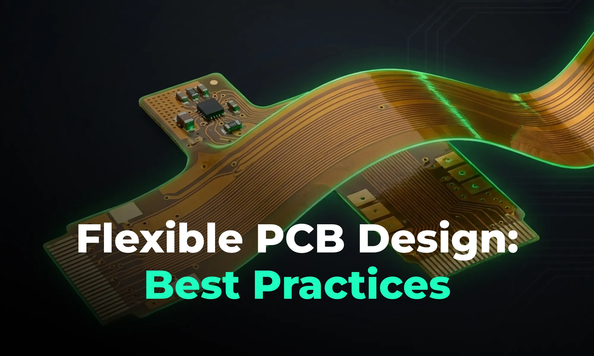
A guide to flexible PCB design, covering materials, stackups, bend radius, and layout best practices for wearables, medical devices, and other compact electronics.

Profile avatar of Yaneev Hacohen
Yaneev Hacohen
|June 8, 2026
How to Read PCB Schematics: A Beginner-Friendly Guide

How to Read PCB Schematics: A Beginner-Friendly Guide

A beginner-friendly guide to reading PCB schematics, covering common symbols, nets, and how to follow signal flow through a circuit diagram.

Profile avatar of Yaneev Hacohen
Yaneev Hacohen
|June 8, 2026
Analog vs Digital PCB Design: Key Differences Explained

Analog vs Digital PCB Design: Key Differences Explained

Learn the key differences between analog and digital PCB design and how to manage mixed-signal layouts for better signal integrity.

Profile avatar of Yaneev Hacohen
Yaneev Hacohen
|May 15, 2026
Decoupling Capacitors in PCB Design: Placement and Selection

Decoupling Capacitors in PCB Design: Placement and Selection

Learn how to place and select decoupling capacitors to improve power integrity in PCB design.

Profile avatar of Yaneev Hacohen
Yaneev Hacohen
|May 15, 2026
Differential Pair Routing: Rules and Best Practices

Differential Pair Routing: Rules and Best Practices

Learn the core rules of differential pair routing including parallel routing, consistent spacing, length matching, and return path management for high-speed PCB designs.

Profile avatar of Yaneev Hacohen
Yaneev Hacohen
|May 15, 2026
PCB EMI Problems: Causes and Solutions

PCB EMI Problems: Causes and Solutions

Learn the most common causes of PCB EMI issues and proven layout, grounding, shielding, and filtering techniques to pass EMC compliance.

Profile avatar of Yaneev Hacohen
Yaneev Hacohen
|May 15, 2026
PCB Testing Methods: Ensuring Quality and Reliability

PCB Testing Methods: Ensuring Quality and Reliability

Learn the most common PCB testing methods including flying probe and in-circuit testing to ensure reliability.

Profile avatar of Yaneev Hacohen
Yaneev Hacohen
|May 15, 2026
Thermal Management in PCB Design: Methods and Best Practices

Thermal Management in PCB Design: Methods and Best Practices

Learn how to manage heat in PCB design with thermal vias, copper pours, layout strategies, and cooling techniques to improve reliability.

Profile avatar of Yaneev Hacohen
Yaneev Hacohen
|May 15, 2026