June 7, 2023
PCB Design: What You Need to Know Before You Start
Share

Throughout this article, I’ll also share with you various strategies and tips for surpassing the obstacles in your path. In today's digital age, where electronic devices have become an integral part of our lives, understanding the intricacies of PCB design is crucial for anyone seeking to create innovative and reliable electronic products.

PCB, short for Printed Circuit Board, is the backbone of virtually every electronic device we encounter today. Your iPhone has multiple of it, your laptop, your noise-cancelling headphones, your big flat tv, your smart watch, everything that are battery-powered devices for sure have one or more inside. PCB is a flat board made of non-conductive material, often fiberglass, with a layer of copper on one or both sides. The copper traces on a PCB act as electrical pathways, connecting various electronic components such as resistors, capacitors, inductors and complicated integrated circuits, and enabling them to work in harmony.
It is the critical bridge between the abstract world of circuitry and the tangible reality of electronic devices. Well-designed PCBs ensure the optimal performance, functionality, and reliability of electronic products. Whether it's a smartphone, a medical device, or a space exploration module, a thoughtfully designed PCB is the key to unlocking the full potential of the underlying electronics.
So, what factors should one consider before stepping into the fascinating world of printed circuit board design? While there are numerous aspects to keep in mind, let's highlight a few crucial ones. First and foremost, electrical performance takes center stage. The PCB design must account for signal integrity, power distribution, and electromagnetic compatibility, to prevent issues like signal degradation, voltage fluctuations, and unwanted interference.

But it doesn't end there. Mechanical aspects also play a vital role in PCB design. The size, shape, and mechanical support of the PCB are crucial factors in ensuring compatibility with the intended enclosure or system. Heat dissipation, component placement, and routing efficiency are all critical in preventing thermal issues and maintaining overall system reliability.
Manufacturability and cost-effectiveness should never be overlooked. Designing a PCB that should be easily fabricated, assembled (does it needs hot-air solder or just solder iron), and tested without compromising quality is essential for efficient production. Considering factors such as the vias spec, trace width and spacing, choice of dielectric materials, cores, component sourcing, and production techniques can significantly impact the overall cost and time-to-market of the final product.
When it comes to PCB design, the software or EDA/CAD you choose plays a vital role in the success of your design process. It can greatly impact the efficiency, accuracy, and overall quality of your final PCB layout. One EDA software that stands out in this regard is flux.ai. It offers a range of innovative features, including a community part library, a hardware AI assistant, and automated impedance control, making it a top contender worth considering.
What sets flux.ai apart is its integration of a hardware AI assistant, Flux Copilot. This advanced feature utilizes artificial intelligence to provide intelligent recommendations and guidance throughout your design journey. It's like having a knowledgeable companion by your side, helping you make informed decisions, optimize your designs, and minimize the chances of errors.
Another impressive feature of flux.ai is its latest feature: automated impedance control. This is particularly important in high-speed designs where maintaining signal integrity is crucial. By automating the impedance control process, flux.ai simplifies the task of achieving precise impedance matching. You just have to look for a component in the community library, add it to the schematic editor, and wire the pins together; then if the system detects you're using a component that needs impedance control - flux.ai will take care of the rest for you. This saves valuable time and effort for designers, allowing them to focus on other critical aspects of their design.
When selecting PCB design software, it's essential to consider your specific design requirements, ease of use, available features, and compatibility with your preferred design methodologies. It's also worth exploring the software's reputation within the industry, the level of community support, and the availability of comprehensive documentation. Altium Designer, Eagle, KiCad, OrCAD, and Proteus are a few examples of PCB design software out there.

At the core of every successful PCB design is the schematic diagram, sometimes called schematic design. It serves as the blueprint, visually representing the electrical connections and components of the circuit board design. A schematic diagram consists of component symbols, net connections between symbols, and netlist. These nets will become the traces on the PCB. The schematic diagram also acts as a common language, facilitating collaboration between engineers, designers, and manufacturers.
A well-designed schematic diagram brings clarity and organization to the circuit, allowing for a comprehensive understanding of its functionality. It also plays a vital role in ensuring electrical integrity by identifying and addressing potential issues early on, reducing the need for costly modifications later.
The schematic diagram serves as a reference point during testing and troubleshooting, enabling engineers to trace the signal flow and pinpoint problem areas. By utilizing standardized symbols and specialized software tools, the design process becomes more efficient and accurate.

In PCB design, layer stackup refers to the arrangement and configuration of the various layers that make up the PCB. It plays a crucial role in determining the performance, functionality, and manufacturability of the final board.
The layer stackup defines the number and type of copper and dielectric layers, their order, and the materials used. It directly impacts important aspects such as signal integrity, power distribution, thermal management, and impedance control. Proper layer stackup design ensures optimal electrical performance, reduces interference, and facilitates efficient routing of traces.
To create an effective layer stackup, designers must consider factors such as the number and types of signal layers, power, and ground planes, and the placement of critical components. The choice of materials for each layer and their dielectric properties is also significant, as it affects impedance matching, signal propagation, and heat dissipation.
By providing predefined layer stackups, Flux simplifies the design process and ensures compatibility with specific PCB manufacturers. The stackups configured for JLCPCB, PCBway, and AISLER, are tailored to their fabrication capabilities, including considerations for board thickness, copper weight, and minimum feature sizes. This facilitates seamless integration between the PCB design and manufacturing processes, streamlining production and reducing potential issues.
When working with flux.ai, designers can leverage the predefined layer stackups to align their design with the requirements of trusted PCB manufacturers. This not only saves time and effort but also enhances the likelihood of successful manufacturing outcomes.
In PCB design, one crucial aspect that greatly impacts the overall performance and manufacturability of the board is component placement. The strategic arrangement of components on the PCB plays a vital role in ensuring optimal functionality, signal integrity, thermal management, and ease of manufacturing and assembly.
Effective component placement starts with careful consideration of the functional requirements and constraints of the design. It involves placing components in such a way that minimizes signal interference, reduces trace lengths, and facilitates efficient routing. Proper component placement can enhance signal integrity by minimizing noise, crosstalk, and electromagnetic interference.
Thermal management is another critical factor to consider during component placement. Components that generate significant heat, such as power amplifiers or microprocessors, should be strategically positioned to allow for effective heat dissipation. Placing heat-sensitive components away from high-temperature sources can prevent overheating and ensure the longevity and reliability of the board.
Manufacturability and assembly considerations also come into play during component placement. Components should be positioned in a manner that allows for easy access during assembly and soldering processes. Adequate clearance and spacing should be provided to accommodate the size and shape of the components, as well as any required test points or connectors.
Coordinating the placement of PCB components with mechanical design elements, such as enclosure dimensions and mounting points, ensures seamless integration between the PCB and the overall product design.
To aid in efficient component placement, most PCB design software provides features like automated placement assistance and 3D visualization. These tools assist in aligning components, optimizing routing, and verifying clearances. However, the human touch and expertise of the designer remain invaluable in making informed decisions based on the specific requirements and constraints of the design.
In the world of PCBs, one critical aspect that demands careful attention and expertise is PCB routing. PCB routing involves the intricate task of connecting components and traces on the board, enabling the smooth flow of signals while considering factors like signal integrity, noise reduction, and manufacturability.
The routing process requires a keen understanding of the design requirements, electrical characteristics, and spatial constraints. Designers must carefully plan the routing strategy, taking into account the complexity of the circuit, signal frequencies, and the importance of signal paths.
To achieve optimal routing, designers must consider signal integrity factors such as trace length matching, impedance control, and minimizing electromagnetic interference. Critical high-speed signals often require controlled impedance routing, differential pair routing, and proper shielding techniques to ensure reliable signal transmission and prevent signal degradation.
Proper power distribution and ground plane design are also essential in PCB routing. By providing a robust power delivery network and a well-designed ground plane, designers can minimize voltage drop, reduce noise coupling, and ensure a stable power supply to all components.
While routing, designers must also consider the physical constraints of the PCB, including component footprints, board size, and mechanical considerations. Components should be placed and routed in a way that facilitates ease of assembly, maintenance, and future modifications if necessary.
Efficient PCB routing involves finding the optimal path for each signal while minimizing crosstalk and maintaining appropriate spacing between traces. Designers may employ routing techniques such as differential pair routing, length tuning, via stitching, and layer stacking to achieve the desired electrical performance.
Determining the appropriate trace width and spacing involves finding a balance between accommodating the current-carrying capacity of the trace, controlling impedance, and ensuring proper insulation between adjacent traces. The trace width refers to the width of the copper conductive path on the PCB. It plays a crucial role in carrying the required current without causing excessive resistance or voltage drop. Selecting the appropriate trace width depends on factors such as the maximum current expected to flow through the trace, the desired temperature rise, and the copper thickness. PCB Designers often refer to standard trace width tables or employ online calculators to determine the optimal trace width for a given current requirement.
Spacing between traces is equally important. It refers to the distance maintained between adjacent traces to prevent unintended coupling, crosstalk, and electromagnetic interference (EMI). Maintaining proper spacing ensures signal integrity and reduces the chances of cross-coupling between adjacent traces.
To establish appropriate trace width and spacing, industry standards and design guidelines are often followed. These standards specify minimum trace widths, spacing requirements, and clearance distances based on factors like signal type, operating frequency, and environmental considerations. Adhering to these guidelines helps ensure compliance with safety regulations and industry best practices.
One vital aspect that demands attention is understanding the design specifications for pads and vias. These elements serve as crucial connection points for integrated circuits, components, traces, and signal paths on the board. Having a thorough grasp of their design specifications is essential for achieving reliable electrical connections, efficient signal routing, and successful manufacturing.
Pads, also known as landing pads or soldering pads, provide the interface between the component leads and the PCB. They play a significant role in ensuring proper soldering, mechanical stability, and electrical connectivity. The design specifications for pads include dimensions such as diameter, shape, and solder mask clearance. These specifications are determined based on the component's footprint, lead size, and manufacturing process requirements.
The shape and dimensions of the pad should match the component's lead style, such as through-hole, surface-mount, or fine-pitch components. Adequate pad size and shape are crucial for achieving reliable solder joints and ensuring mechanical strength. The solder mask clearance around the pad helps to prevent solder bridging or short circuits during assembly.
Vias, on the other hand, are conductive pathways that connect different layers of the PCB. They enable the transfer of signals, power, and ground between different parts of the circuit. The design specifications for vias include parameters such as diameter, aspect ratio, and annular ring size.
There are different types of vias in PCB; through-hole via, blind via, buried via, and micro via. Through-hole vias are more common. Read more about different types of PCB vias.
The diameter of a via determines its electrical and thermal characteristics. It should be appropriately sized to handle the required current and ensure low-resistance connections. The aspect ratio, defined as the ratio of the via's depth to its diameter, affects the manufacturability and reliability of the via. Adequate aspect ratios are necessary to ensure proper plating and maintain structural integrity during the fabrication process.
The annular ring, which refers to the copper pad surrounding the via, is essential for maintaining the electrical connection between the via and the pad or trace. Sufficient annular ring width is necessary to ensure reliable electrical connectivity and prevent potential shorts or open circuits.

Gerber files are a collection of ASCII-based data files that describe the various layers, copper traces, pads, holes, and other design elements of the PCB.
When the PCB design is complete and ready for manufacturing, the design files are converted into Gerber files. These files provide a detailed representation of each layer of the PCB, including the top and bottom copper layers, solder mask layers, silkscreen layers, and drill files.
Gerber files are typically generated by the PCB design software used to create the layout. Each layer of the PCB design is exported as a separate Gerber file, with a specific extension that identifies the layer. The most common Gerber file extensions include .GTL (Top Layer), .GBL (Bottom Layer), .GTS (Top Solder Mask), .GBS (Bottom Solder Mask), .GTO (Top Silkscreen), .GBO (Bottom Silkscreen), and . TXT (Drill Files).
These Gerber files act as a bridge between the PCB designer and the PCB manufacturer. They contain all the necessary information required for the fabrication process, such as the dimensions, copper traces, solder mask openings, component placement locations, and drill hole positions.
Once the Gerber files are created, they are typically bundled together and submitted to the PCB manufacturer for the manufacturing process. The manufacturer uses the Gerber files to generate the photolithographic films or digital equivalents that are used in the fabrication steps, including the creation of the copper layers, solder mask application, silkscreen printing, and drilling of holes.
The BOM specifies the quantity of each component required for the PCB assembly, enabling accurate procurement and inventory management. The reference designator assigns a unique identifier to each component on the PCB, facilitating proper placement and soldering during the assembly process.
Finding a reliable and suitable manufacturer ensures the successful fabrication of your PCB design.
Choosing the right PCB manufacturer involves considering several factors. Here are a few key points to keep in mind:
So, are you ready to take the first step towards your PCB project? Turn your ideas into tangible circuit boards that can make a difference whether it's for your hydronics system, automated curtain opener, IoT-based projects or designing hardware for the next SpaceX mission, Flux is where great hardware projects are born. Get started now for free!


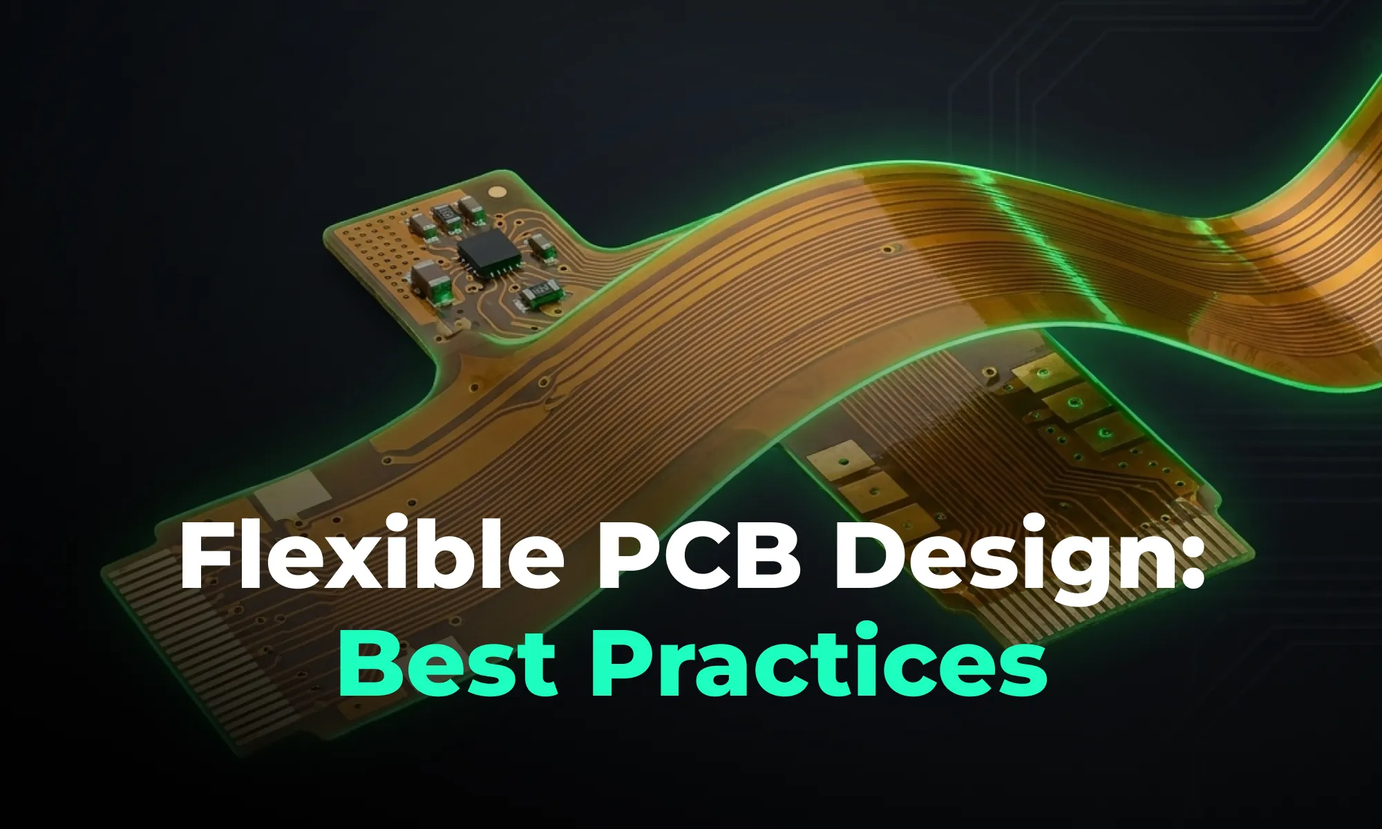
A guide to flexible PCB design, covering materials, stackups, bend radius, and layout best practices for wearables, medical devices, and other compact electronics.

A beginner-friendly guide to reading PCB schematics, covering common symbols, nets, and how to follow signal flow through a circuit diagram.

An overview of collaborative PCB design, showing how cloud-native tools, real-time editing, and shared libraries are reshaping modern hardware team workflows.

A guide to managing PCB component libraries, covering symbols, footprints, and 3D models with best practices for standardizing parts across hardware teams.

An overview of PCB reverse engineering, explaining how engineers analyze boards, extract schematics, and use the process for legacy support, repair, and design analysis.
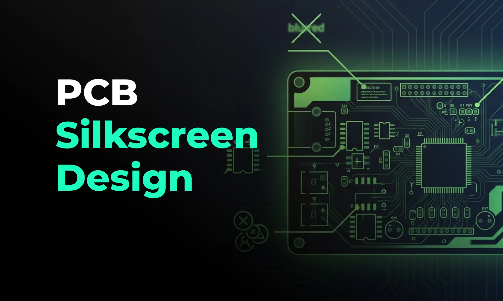
A practical guide to PCB silkscreen design, covering labeling best practices, common readability mistakes, and how clean silkscreens improve assembly and debugging.

An explainer on PCB version control, comparing hardware revision workflows to Git-style collaboration and showing how modern teams track design changes.
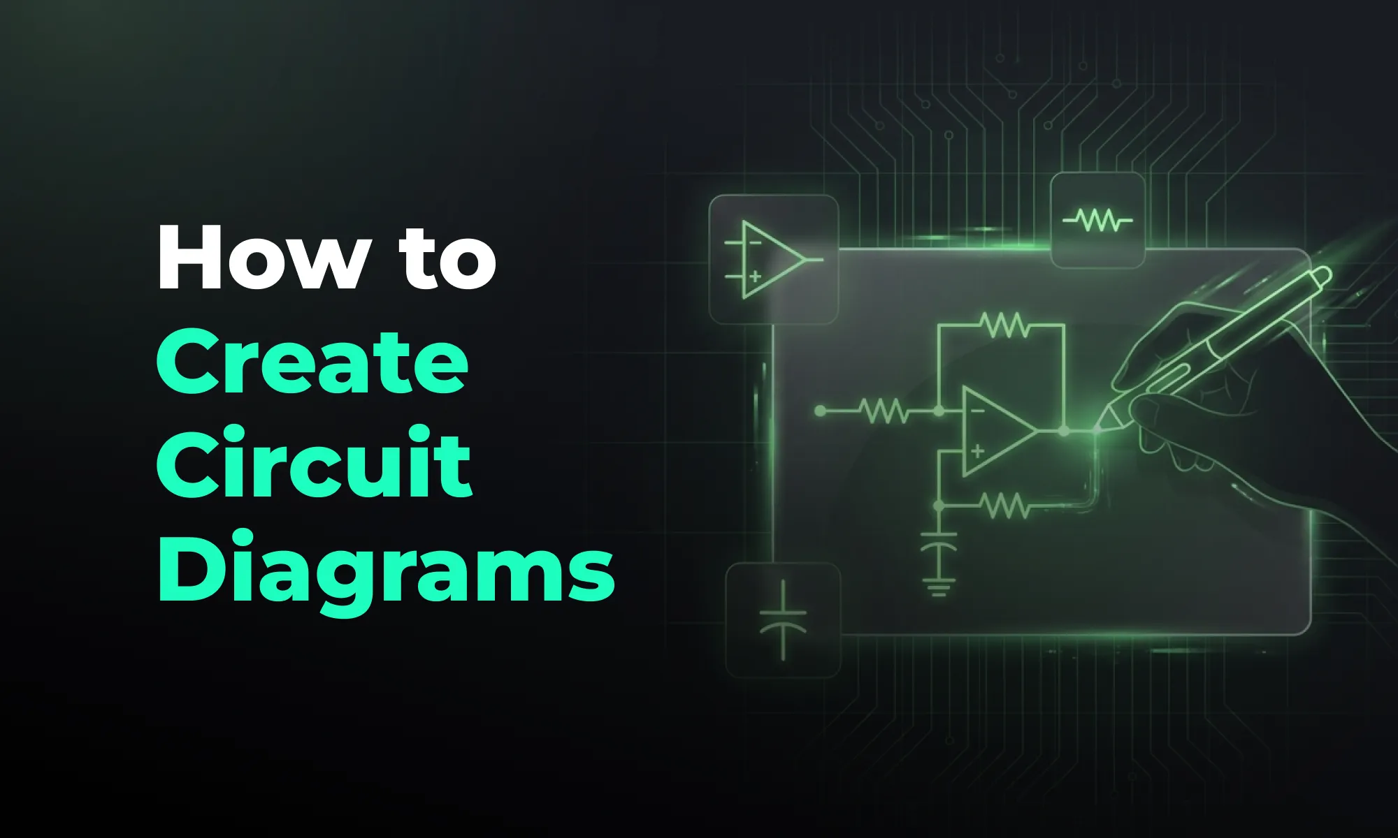
An introduction to schematic capture, explaining how engineers use symbols, nets, and connectivity to create circuit diagrams that drive PCB layout.
