Flux Blog

News, resources, and company updates

Meet Files: AI-Native Project Documentation

Files is a new top-level tab in Flux projects that centralizes all project documentation, including specs, uploaded assets, generated outputs, and project descriptions, in one place. This gives Flux full access to your project context, enabling better outputs, continuity across sessions, and easier team collaboration.

|
April 16, 2026
Thank you! Your submission has been received!
Oops! Something went wrong while submitting the form.
PCB Design for Manufacturability (DFM): Rules and Best Practices

PCB Design for Manufacturability (DFM): Rules and Best Practices

Design for Manufacturability (DFM) is the essential practice of optimizing your PCB layout to ensure accurate and cost-effective assembly, so how can you ensure you avoid the costly re-spins and low production yields caused by ignoring manufacturing limits?

A printed circuit board (PCB) that functions flawlessly in a digital simulation is useless if a fabrication house cannot physically build it. Bridging the gap between the theoretical schematic and the physical production line requires adherence to PCB Design for Manufacturability (DFM).

DFM is the practice of designing your board to be manufacturable based on the physical capabilities and tolerances of modern manufacturing equipment. Failing to follow DFM guidelines results in expensive board re-spins, delayed product launches, and high defect rates. This guide breaks down the core DFM principles, common production pitfalls, and the exact rules you need to follow to ensure your layout is ready for the factory floor.

Key Takeaways

  • DFM bridges the gap between design and production: PCB Design for Manufacturability (DFM) ensures your digital layout perfectly aligns with the physical limits of chemical etching, drilling, and assembly equipment.
  • Ignoring DFM leads to costly delays: Failing to adhere to manufacturability rules results in expensive board re-spins, low production yields, and missed project deadlines.
  • Strict rules govern trace, via, and pad geometries: Following manufacturer-provided constraints for trace width, clearance, and annular rings prevents common fabrication defects.
  • DFM goes beyond standard rule checking: While DRC verifies that software constraints are met, DFM is a holistic review ensuring the board can actually be built and assembled reliably in the real world.
  • Modern EDA tools prevent errors early: Cloud-native platforms like Flux integrate real-time validation and collaborative reviews to catch manufacturing issues long before the board is sent to the fab house.

What Is PCB Design for Manufacturability (DFM)?

DFM stands for Design for Manufacturability. In the context of hardware engineering, it is the process of optimizing your PCB layout so that it can be fabricated and assembled as easily, reliably, and cost-effectively as possible.

While you might be able to draw a 2-mil (0.05mm) trace in your CAD software, a standard manufacturer's etching process might over-etch and dissolve that trace entirely, creating a broken circuit. PCB DFM involves understanding the physical and chemical limits of the circuit board production process, from copper etching and mechanical drilling to robotic pick-and-place assembly, and applying those limits to your layout as PCB design constraints.

Why DFM Is Critical in PCB Design

Ignoring design for manufacturability PCB principles has severe financial and operational consequences.

  • Cost of Board Re-Spins: A "re-spin" happens when a board is manufactured, fails testing due to a design flaw, and must be redesigned and re-manufactured. A single re-spin can cost thousands of dollars in wasted materials and Non-Recurring Engineering (NRE) fees.
  • Production Delays: Fabricating and assembling a complex board can take 2 to 4 weeks. If a DFM error forces a re-spin, your project timeline is instantly delayed by a month.
  • Yield Issues: "Yield" is the percentage of manufactured boards that function correctly. A layout that pushes manufacturing tolerances to their absolute limits might have a yield of only 60%. This means 40% of the boards must be thrown away, drastically increasing the price-per-unit of the functional boards. DFM ensures a yield close to 100%.

Key PCB Manufacturability Rules

To ensure a smooth transition from design to production, engineers must adhere to standard PCB manufacturing guidelines. Before starting a layout, always check your specific manufacturer's capabilities sheet.

Trace Width and Spacing

Manufacturers have limits on how thin a trace can be and how close two traces can sit (often referred to as "trace/space"). A standard cost-effective rule is 6/6 mil (6 mil trace width, 6 mil spacing), while advanced high-density boards might push to 4/4 mil or 3/3 mil.

Via Sizes and Drill Constraints

Drill bits have physical limits. A key metric is the aspect ratio (the board thickness divided by the drilled hole size). A safe industry standard is a 10:1 aspect ratio. Additionally, you must ensure a sufficient annular ring (the ring of copper surrounding the drilled hole) so that if the drill bit wanders slightly during manufacturing, it doesn't break outside the copper pad.

Component Spacing

Component spacing prevents pick-and-place machine nozzles from knocking adjacent parts during assembly. It also ensures ensures there’s enough room for soldering irons or rework tools to access the pins.

Solder Mask Clearances

Solder mask requires a slight expansion around copper pads to account for registration tolerances (misalignment during printing). If the expansion is too small, the soldermask might cover the pad, preventing solder from sticking. Furthermore, maintain a minimum "web width" of solder mask between closely spaced pads to prevent solder from bridging them together during reflow.

Common PCB DFM Issues

Even experienced engineers can overlook physical constraints. To help you identify risks during your layout phase, here is a breakdown of the most common PCB production issues caught during DFM reviews:

DFM Issue Cause Manufacturing Consequence Solution
Acid Traps Traces routed at acute angles (less than 90 degrees). Etching chemicals pool in the corner, over-etching and breaking the trace. Always route traces at 45-degree angles or use curved routing.
Solder Bridging Insufficient trace-to-pad clearance or missing solder mask webbing. Solder melts across two adjacent pads during reflow, creating a dead short. Adhere to manufacturer minimum spacing and solder mask expansion rules.
Drill Breakout Specifying an annular ring that is too small for the fab house's drill tolerance. The drill bit wanders outside the copper pad, severing the layer-to-layer connection. Increase via pad sizes to guarantee a robust annular ring around the drilled hole.
Tombstoning Uneven thermal mass on a two-pin component (e.g., one pad connected to a thin trace, the other to a massive ground plane). Solder melts unevenly, pulling the component upright like a tombstone and breaking the circuit. Use thermal relief spokes when connecting SMD pads to large copper planes.
Cracked Components Placing fragile parts (like ceramic capacitors) too close to board edges or V-score lines. Mechanical stress during board depanelization causes the component body to fracture. Maintain a strict keep-out zone (e.g., 50–100 mils) near all board edges.

PCB DFM Checklist

To avoid the PCB DFM errors mentioned above, run through this DFM PCB checklist before generating your manufacturing files:

  • Follow spacing rules: Verify all trace-to-trace, trace-to-pad, and pad-to-pad clearances meet your manufacturer's minimum requirements.
  • Validate drill sizes: Ensure your smallest drill hole does not exceed the manufacturer's maximum aspect ratio, and verify adequate annular rings on all vias.
  • Ensure component clearances: Check 3D courtyards to ensure components do not physically overlap and have sufficient clearance for assembly nozzles.
  • Review solder mask: Confirm adequate solder mask expansion around pads and check for minimum solder mask webbing between fine-pitch IC pins.
  • Check thermal relief: Ensure thermal relief spokes are used when connecting surface-mount pads or through-holes to large copper planes to prevent tombstoning and cold solder joints.
  • Verify edge clearance: Keep all copper traces and components at least 50 to 100 mils away from the board edge.

DFM vs DRC: What’s the Difference?

These two terms are often used together, but they serve different purposes in the PCB layout for manufacturing workflow:

  • DRC (Design Rule Checking): This is a rigid, software-driven pass/fail check. It verifies whether your layout obeys the exact constraints you programmed into the software (e.g., "Are all traces exactly 5 mils apart?").
  • DFM (Design for Manufacturability): This is a holistic evaluation of how buildable the board is. A board can perfectly pass a DRC but still fail a DFM check. For instance, a trace routing perfectly 5 mils away from a pad passes DRC, but if it routes at a sharp, acute angle, it creates an "acid trap" that fails DFM because it will over-etch in the chemical bath.

How Modern PCB Tools Improve Manufacturability

Historically, DFM was a disjointed process. Engineers would finish a layout, export the files, email them to a manufacturer, and wait days for a DFM report to come back filled with errors.

Modern, cloud-native platforms like Flux eliminate this friction by integrating PCB manufacturability rules directly into the design phase.

By utilizing real-time DRC, Flux prevents designers from making unmanufacturable routing decisions the moment they occur. If you attempt to place a via with an insufficient annular ring, the software flags it instantly. Furthermore, because Flux is a collaborative, browser-based platform, engineers can invite manufacturing partners directly into the design file for collaborative design reviews. Instead of emailing ZIP files back and forth, the fab house can highlight a problematic trace directly on the canvas, drastically accelerating the iteration cycle and ensuring the board is ready for flawless production on day one.

FAQs

What is DFM in PCB design?
Design for Manufacturability (DFM) in PCB design is the practice of optimizing a circuit board layout to ensure it can be fabricated and assembled accurately, efficiently, and cost-effectively by a manufacturer's physical machinery.
Why is manufacturability important?
Manufacturability is critical because it dictates the yield and cost of your board. Designing outside of standard manufacturing tolerances leads to broken traces, short circuits, low production yields, and expensive board re-spins.
What are common PCB DFM issues?
Common DFM issues include inadequate trace spacing leading to shorts, missing thermal reliefs causing tombstoning during assembly, insufficient annular rings causing via breakout, and placing components too close to the board edge.
How do you ensure a PCB can be manufactured?
To ensure manufacturability, you must obtain your chosen fabricator's capability guidelines before routing, program those limits into your software's constraints, run continuous Design Rule Checks (DRC), and perform a final DFM audit covering solder masks, drill sizes, and copper clearances.
What tools help with PCB DFM?
All professional Electronic Design Automation (EDA) software includes rule-checking capabilities. Modern platforms like Flux improve this by offering real-time, continuous design rule validation and cloud-based collaboration, allowing engineers and manufacturers to review board manufacturability concurrently.
|
April 16, 2026
Best PCB Routing Techniques for Clean Circuit Board Layouts

Best PCB Routing Techniques for Clean Circuit Board Layouts

Ready to put these PCB routing techniques into practice? Whether you're dealing with delicate differential pairs or complex multilayer stackups, tedious manual routing and end-of-process DRC checks can slow your whole team down. Upgrade your workflow with Flux, where AI-assisted layout and real-time design rule checks help you build cleaner, more reliable circuit boards faster.

Key Takeaways

  • Follow Core Geometric Rules: Apply the 3W rule for trace spacing, maintain continuous ground planes for a low-impedance return path, and use 45-degree bends or smooth arcs instead of 90-degree corners to prevent localized capacitance increases and signal reflections.
  • Avoid Common Routing Pitfalls: Prevent signal degradation by keeping high-speed signals away from split planes, properly spacing vias to avoid ground plane voiding, and separating analog and digital return currents.
  • Use Modern Tools: Platforms like Flux offer automated routing assistance to catch clearance violations the moment you draw a trace.

What Is PCB Routing?

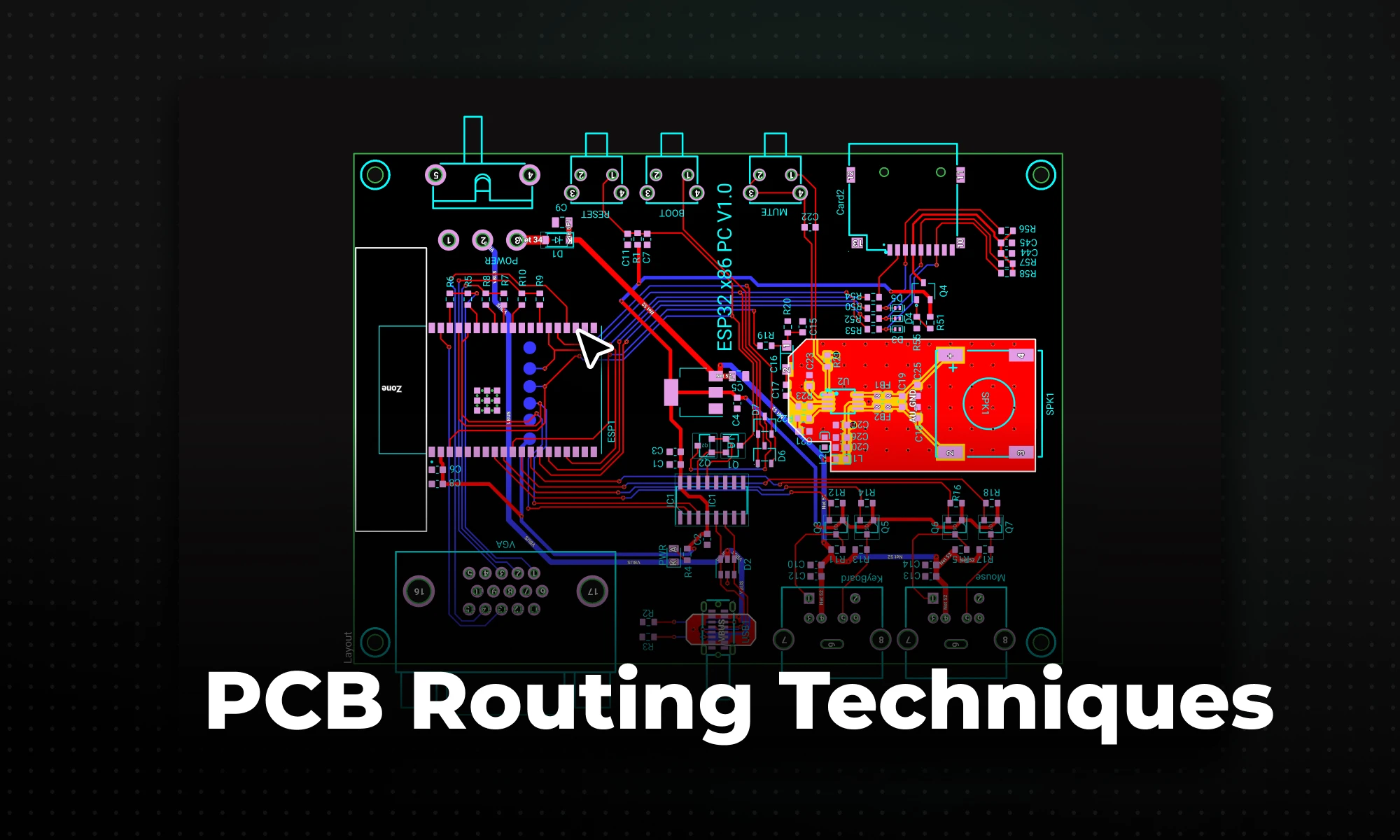
PCB routing is the geometric translation of schematic connectivity on a printed circuit board: the process of drawing copper traces to connect component pads, power sources, and ground planes according to the logical netlist generated during schematic capture. It transforms an abstract electrical design into a manufacturable physical layout.

Routing occurs after component placement and before manufacturing prep. Where it sits in the workflow matters: every decision you make during placement will either constrain or free up your routing options later. The quality of your routing dictates how well the board performs electrically, thermally, and mechanically, and a poor layout can undermine an otherwise sound design.

Why PCB Routing Is Critical for Circuit Board Performance

Treating routing as "connecting the dots" is a fast track to failed prototypes. Trace geometry, layer stackup, and spatial placement directly impact signal integrity, electromagnetic interference (EMI), and power delivery. The physical dimensions of a trace dictate its resistance and inductance, which in turn govern how power and high-frequency signals behave across the board.

Poor routing fails in predictable ways:

  • Crosstalk: Closely routed high-speed traces can couple energy between an aggressor and a victim trace, causing false triggering or data corruption.
  • IR drop and overheating: When current flows through the inherent resistance of a copper trace, it causes a voltage loss known as an IR drop (Current × Resistance). Undersized power traces exacerbate this drop and generate excess heat under heavy loads, which severely degrades board reliability.
  • EMI radiation: Traces routed too close to board edges can act as antennas. Keeping high-speed traces at least 10–15 mils from board edges is standard practice to reduce this leakage.
  • Manufacturing failures: Geometry violations, acute angles, insufficient clearances, can produce shorts, broken traces, or compliance test failures before the board ever powers on.

Core PCB Routing Principles

Every functional PCB layout depends on a set of geometric rules that exist for good reasons. Some are about physics; others are about manufacturability. Knowing which is which helps you apply them intelligently rather than reflexively.

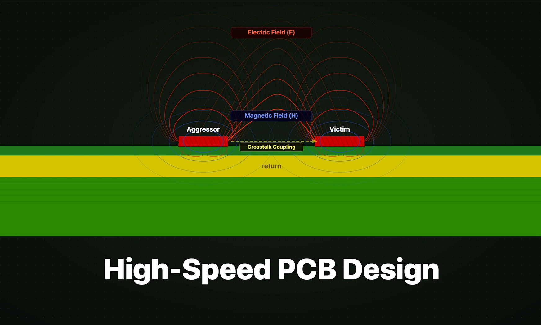
The 3W Rule is the most universal guideline for crosstalk mitigation: the center-to-center distance between two adjacent traces must be at least three times the width of a single trace. This limits the electromagnetic coupling between signal lines.

Trace angles require some nuance. The industry has always said "never use 90-degree bends," but the reality is more qualified. One of the longest-running myths in signal integrity is the requirement to eliminate 90-degree turns in PCB traces, and as time has gone on, this claim has steadily been pushed off to higher and higher frequencies. For engineers, right-angle PCB traces are of practical concern only when the circuit board has to handle high-frequency signals at hundreds of GHz. That said, in traditional etching, a sharp 90-degree internal corner can trap etching acid, leading to over-etching and a potentially thin or broken trace. Modern PCB manufacturing processes have largely mitigated this, but it remains a best practice to avoid them for high-reliability designs. The real rule: avoid acute angles outright (they are genuine acid trap culprits), and default to 45-degree bends as a clean, broadly compatible routing style.

Clearances are voltage-dependent, not arbitrary. The minimum trace spacing depends on the voltage between conductors and their location. Based on IPC-2221 standards, low-voltage signals (0–30V) dictate specific minimum clearances:

  • Internal layers: 0.05 mm (2 mils) minimum spacing.
  • External uncoated conductors: 0.1 mm (4 mils) minimum spacing.

These values increase significantly with voltage, i.e. at 300V, external uncoated conductors require 1.25mm spacing.

IPC-2221 Baseline Clearance Reference (Low-Voltage, External Uncoated Conductors)

Voltage Range Min. Clearance (External, Uncoated) Notes
0–15V 0.05mm (2 mil) Internal layers
0–30V 0.1mm (4 mil) External, uncoated, sea level
30–50V 0.6mm (24 mil) Scales up rapidly
100–150V 1.5mm (59 mil) Consult Table 6-1 directly
>500V Per-volt formula applies See IPC-2221C Table 6-1

Always reference the current IPC-2221C standard (2023 revision) for your specific conductor configuration and altitude.

Essential PCB Routing Principles

  • Minimize trace lengths, especially for high-speed and analog signals.
  • Maintain adequate spacing between traces (apply the 3W rule for signal traces).
  • Avoid unnecessary vias. Each one introduces parasitic inductance and a potential impedance discontinuity.
  • Route high-speed signals away from noisy power supplies and board edges.
  • Provide a solid, continuous ground plane immediately adjacent to high-speed signal layers.
  • Never use acute-angle bends; use 45-degree routing as your default.

Advanced PCB Routing Techniques

When basic rules aren't enough, high-speed digital, RF, DDR memory, mixed-signal, specialized techniques are required to maintain signal integrity at the physical layer.

Differential pair routing is mandatory for interfaces like USB, PCIe, HDMI, and Ethernet. Managing these traces requires strict adherence to geometry:

  • Maintain strict symmetry: Symmetrical routing ensures equal propagation delays and prevents differential signals from converting into common-mode noise.
  • Control intra-pair skew: Length differences between positive and negative traces cause phase misalignment at the receiver, degrading the eye diagram and increasing jitter. High-speed interfaces like PCIe typically demand an intra-pair length tolerance of ±5 mils.
  • Monitor inter-pair skew: For multi-lane interfaces, timing mismatches across different pairs must stay within the specified interface budget.
  • Minimize uncoupled segments: Component breakouts, vias, and connector fan-outs naturally force traces apart. Keep these uncoupled stubs under 2–3 mm before re-coupling the pair.

Daisy-chain (fly-by) routing is the correct topology for connecting multi-drop bus topologies (such as parallel memory architectures). Routing to each device in sequence, rather than branching, keeps stub lengths short and prevents the reflections that branch topologies cause.

Power distribution network (PDN) design has largely moved away from thick power traces toward dedicated, continuous power and ground planes in multilayer stackups. Adjacent power and ground planes in a layer stack provide built-in inter-plane capacitance and significantly lower PDN impedance — a benefit that no amount of discrete decoupling can fully replicate.

Common PCB Routing Mistakes

Even experienced engineers make spatial and layer-management mistakes that degrade board performance. These are the ones that show up repeatedly on failed boards.

Routing over split ground planes is the most damaging. Routing high-speed or sensitive signals across split planes breaks the return current path, creating loop discontinuities and impedance mismatches, which can lead to EMI radiation, signal distortion, and even ground bounce in mixed-signal or power-dense designs. The return current doesn't disappear. It takes the longest available path, and that loop area radiates.

Via voiding in ground planes occurs when vias are packed too tightly in BGA breakouts or connector arrays. When anti-pads (the circular clearance voids in a reference plane that prevent a passing via from shorting to that layer) merge, they create a continuous slot in the internal copper plane, effectively severing the return path. Space vias at least 15 mils apart to preserve the copper webbing between them.

Poor analog/digital separation routinely dooms mixed-signal boards. Digital return currents must never be allowed to flow through the analog section of a reference plane. Routing must physically partition these zones, with a single, controlled crossing point if the two domains must share a plane.

Ignoring voltage-dependent clearances is a beginner mistake that experienced engineers still make when moving between design domains. Failing to account for voltage differences between traces can cause arcing, so always check the standard's clearance tables for your specific voltage levels.

How Modern PCB Tools Improve Routing Workflows

Legacy desktop Electronic Design Automation (EDA) tools force engineers into slow, sequential workflows: route manually, run a batch DRC at the end, find violations, fix them, repeat. For complex multilayer designs, this loop is expensive. Modern, cloud-native platforms eliminate much of that friction.

Flux provides an environment where schematic-to-layout synchronization is continuous and collaborative — no manual back-annotation, no file handoffs. Instead of catching IPC-2221 spacing violations at the end of a design phase, real-time DRC flags them the moment you draw the trace. Flux also integrates automated routing assistance and AI-assisted routing tools that help engineers iterate through placement and routing options faster, reserving manual attention for the high-speed signals that actually require it.

The practical result: engineering teams spend less time wrestling with the tool and more time solving the actual design problem.

FAQs

What is PCB routing?
PCB routing is the process of mapping physical copper traces on a circuit board to connect components electrically, based on the logical connections defined in the schematic. It follows component placement and directly determines the board's electrical performance and manufacturability.
What are the best PCB routing techniques?
Keep traces as short as possible, default to 45-degree bends over 90-degree corners, maintain continuous ground reference planes, and apply the 3W rule for trace spacing. For high-speed designs, differential pair routing with tight length matching and controlled impedance should be used.
How do engineers route traces on a PCB?
Engineers use EDA software to place traces layer by layer, managing width for current capacity and spacing for signal integrity. Vias transition signals between layers; design rule checks validate clearance and impedance requirements throughout the process.
What is differential pair routing?
Differential pair routing involves routing two complementary signals in parallel with matched lengths and symmetrical spacing. Differential pairs consist of two closely coupled traces carrying complementary signals, which inherently reject common-mode noise and enable higher bandwidth. It's required for interfaces like USB, PCIe, HDMI, and Ethernet.
What software is used for PCB routing?
Engineers use EDA platforms ranging from legacy desktop tools like Altium and Cadence to modern, cloud-collaborative platforms like Flux, which offer real-time DRC and AI-assisted routing workflows. The right tool depends on design complexity, team size, and how much you value integrated collaboration.
|
April 16, 2026
Design Rule Checking (DRC) in PCB Design: Real-Time vs Batch, Rules, and Common Failures

Design Rule Checking (DRC) in PCB Design: Real-Time vs Batch, Rules, and Common Failures

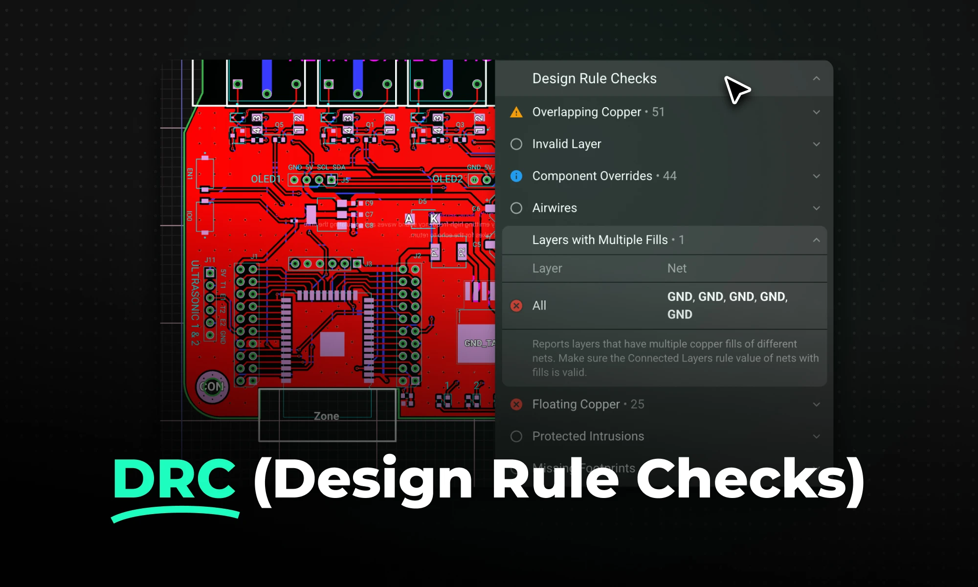
DRC is an automated process that checks your PCB layout against manufacturing and electrical constraints, catching errors like trace spacing and drill sizes before fabrication. Modern tools run this in real-time during design, while older ones batch-check at the end, often producing overwhelming error lists.

Key Takeaways

What Are Design Rule Checks (DRC) in PCB Design?

Design Rule Checking (DRC) is an automated verification process within Electronic Design Automation (EDA) software that ensures a circuit board layout complies with a predefined set of geometrical and electrical constraints.

Before a board is sent to a manufacturer, it must pass a PCB design rule check (DRC), which ensures the design complies with the manufacturer’s physical limitations in etching, drilling, and routing. For example, a standard fabrication house might have a minimum manufacturing tolerance of a 4-mil trace width and a 4-mil spacing gap. If you design a board with 3-mil traces, the manufacturer physically cannot produce it reliably.

By configuring your PCB manufacturing design rules upfront, DRC constantly scans the layout to catch errors, ensuring that elements like trace widths, copper clearances, and via geometries are safely within manufacturable limits. Catching a clearance violation in software costs nothing; finding out about it after ordering a batch of 500 boards is a costly disaster.

Types of PCB Design Rules

To effectively design a layout, engineers must configure various categories of PCB design rules. These constraints are typically derived from industry standards (like IPC-2221) and the specific capabilities of your chosen manufacturer.

The most common rule categories include:

  • Trace Width Constraints: Dictates the minimum and maximum thickness of a copper trace. This is crucial for current carrying capacity (power traces must be wider) and impedance control.
  • PCB Clearance Rules: Defines the minimum allowable distance through the air or across the surface of the board between two different copper elements (e.g., trace-to-trace, trace-to-pad, or pad-to-via) to prevent electrical arcing and short circuits.
  • Component Spacing (Courtyards): Ensures physical components are not placed so close together that they collide during robotic pick-and-place assembly.
  • Drill and Via Size Rules: Establishes the minimum hole size a mechanical drill or laser can create, as well as the minimum annular ring (the copper pad surrounding the drilled hole) required to prevent drill breakout.
  • Solder Mask Rules: Defines the minimum expansion of the solder mask opening around a pad and the minimum "webbing" (the sliver of solder mask between two close pads) to prevent solder bridges during assembly.

PCB Design Rule Checklist

Before beginning your layout or running a final check, verify you have configured constraints for:

  • Minimum trace width
  • Trace-to-trace clearance
  • Trace-to-pad clearance
  • Minimum via drill size and annular ring
  • Component courtyard spacing
  • Solder mask expansion and sliver limits
  • Silkscreen-to-pad clearance (ensuring ink doesn't cover solderable areas)

Real-Time vs Batch Design Rule Checking

Historically, PCB layout rule checks were handled as an afterthought. Today, modern workflows have shifted how these checks are executed.

Batch DRC

In legacy desktop EDA tools, engineers typically route large sections of the board—or even finish the entire layout—before manually clicking a "Run DRC" button. This is known as Batch DRC.

The problem with batch DRC: Running a batch DRC at the end of a design phase often results in a massive, overwhelming list of hundreds of errors. Fixing a trace spacing issue found via a batch check might require you to rip up and reroute a massive section of a dense board, wasting hours of engineering time.

Real-Time DRC

Modern PCB design platforms employ Real-Time DRC (or online DRC). In such a workflow, the software's rules engine runs constantly in the background.

The advantage of real-time DRC: Errors are detected during the layout process. If you attempt to draw a trace too close to a via, the software instantly flags the violation visually or actively prevents you from placing the invalid segment. This immediate feedback prevents errors from cascading, drastically reducing design iteration time and eliminating the dreaded "end-of-project error log."

Common PCB DRC Errors Engineers Encounter

Even with meticulous planning, engineers frequently encounter design rule check (DRC) violations during PCB layout. These errors typically occur when the physical layout conflicts with electrical or manufacturing constraints defined in the design rules. Recognizing the most common violations helps engineers identify and resolve problems quickly before manufacturing. Such common violations include trace clearance issues, overlapping copper features, incorrect trace widths, via aspect ratio problems, and component spacing conflicts.

DRC Violation Description
Trace Clearance Violations Occurs when a trace is routed too close to another trace, pad, or via belonging to a different net, risking electrical shorts or signal interference.
Overlapping Copper Features Happens when vias, pads, or traces overlap, unintentionally connecting different signals and creating short circuits.
Incorrect Trace Width Occurs when a trace narrows below the defined minimum width, often when transitioning from a wide power plane through tight pin spacing.
Via Size Violations (Aspect Ratio) Arises when the drill hole of a via is too small relative to the board thickness, exceeding manufacturing aspect-ratio limits.
Component Spacing Issues Happens when component bodies or defined courtyards overlap, meaning the parts cannot be physically assembled on the board.

How DRC Prevents Manufacturing Failures

The ultimate goal of a design rule check PCB workflow is bridging the gap between digital theory and physical manufacturing. By rigorously enforcing rules, DRC ensures:

  • Manufacturability (DFM): If your board fails fabrication limits, the fab house will place your order on "engineering hold," delaying your project. DRC ensures your design matches the manufacturer's capabilities.
  • Reliable Board Assembly (DFA): Enforcing solder mask webbing rules prevents "solder bridging"—where solder accidentally connects two adjacent pins during reflow, creating a short. Enforcing component spacing allows assembly machines to place parts without knocking neighboring chips off the board.
  • Electrical Reliability: Maintaining proper clearances prevents high-voltage arcing. Ensuring minimum trace widths prevents power lines from acting like fuses and burning up under high current loads. Properly sized annular rings prevent vias from cracking and breaking connections during thermal expansion.

(For deeper insights on planning highly reliable boards, explore our multilayer PCB design tutorial.)

How Modern PCB Tools Improve Design Rule Checking

Traditional EDA tools often treat design validation as a slow, batch-processed hurdle at the end of a project. Modern, cloud-native platforms like Flux flip this script by weaving validation directly into the active drafting process. By shifting from reactive troubleshooting to proactive guidance, modern tools improve the DRC workflow in several key ways.

Flux: Collaborative, Browser-Based Electronics Design

Flux is a modern EDA platform built for the way hardware teams actually work today, in the browser, collaboratively, and with tight schematic-to-PCB integration.

  • Real-Time DRC Validation The rules engine operates continuously in the background, providing instant visual cues the exact moment a trace or component violates a manufacturing constraint.
  • Automatic Rule Enforcement Interactive routing features actively prevent designers from making invalid moves, keeping the layout strictly within fabrication limits at all times.
  • Faster Layout Iteration Because issues are caught and resolved in milliseconds as they happen, engineers no longer have to spend days untangling a web of cascading errors at the end of a project.
  • Collaborative Design Review Flux's "multiplayer" environment eliminates siloed, desktop-bound data. If a complex rule violation occurs, an engineer can instantly share a live link to the exact error with a colleague or fabricator to troubleshoot together—no zip files, PDFs, or lengthy emails required.

Ultimately, this combination of real-time feedback and collaboration reduces the risk of costly manufacturing errors. By ensuring every routing decision complies with fabrication limits the moment it is made, modern platforms prevent unmanufacturable designs from ever reaching the fab house, eliminating unnecessary board re-spins and maintaining tight project schedules.

FAQs

What is design rule checking in PCB design?
Design Rule Checking (DRC) is an automated verification process used in PCB design software to ensure the board layout adheres to specific electrical and physical manufacturing constraints. It acts as a final audit to catch human errors before fabrication.
Why is DRC important in PCB layout?
DRC is critical because it prevents unmanufacturable designs from being sent to the fabrication house. By verifying minimum trace widths, clearances, and drill sizes, it eliminates the risk of short circuits, assembly failures, and costly board re-spins.
What are common PCB DRC errors?
The most common PCB DRC errors include trace-to-trace clearance violations, trace width minimum violations, overlapping component courtyards, and insufficient annular rings on vias.
What is the difference between real-time and batch DRC?
Batch DRC is run manually after a large portion of the layout is complete, often resulting in a long, difficult-to-manage list of errors. Real-time DRC runs continuously in the background, providing immediate visual feedback and preventing the designer from making invalid routing moves as they happen.
What software performs PCB design rule checking?
Almost all Electronic Design Automation (EDA) software performs DRC. While legacy desktop tools typically rely on batch DRCs, modern, browser-based platforms like Flux integrate sophisticated, real-time DRC engines that provide instant feedback during the layout process.
|
March 26, 2026
High-Speed PCB Design: Layout Rules, Signal Integrity, and Routing Best Practices

High-Speed PCB Design: Layout Rules, Signal Integrity, and Routing Best Practices

Whether you're migrating from popular EDA applications or starting fresh, mastering high speed PCB design has never been more intuitive. Flux enables teams to design, simulate, and route with real-time AI assistance, so you can spin your next high-speed board with total confidence.

Key Takeaways

What Is High-Speed PCB Design?

The most common misconception: a board only becomes "high-speed" once the system clock crosses some ultra-high threshold. That's wrong, and it's expensive to learn the hard way.

High-speed design becomes necessary when the signal's rise time approaches a critical threshold where transmission line effects become significant — specifically, when the signal rise time is less than four times the propagation delay. At that point, your copper traces stop acting as simple wires and start behaving as transmission lines. A transmission line is a distributed waveguide that directs high-frequency alternating currents; if you route or terminate it improperly, it functions as an accidental antenna, radiating electromagnetic interference across your entire board. Because of this, you must actively control characteristic impedance, mitigate reflections, and secure the return path.

Two practical rules of thumb help identify when you're in this territory:

  • If the highest frequency content in your signals exceeds 50 MHz, you should treat it as a high-speed design (though there are edge cases where 60 MHz may not require it, and some 40 MHz designs may).
  • If an interconnection length reaches or exceeds λ/12 (one-twelfth of the signal's wavelength in the PCB medium), it must be treated as a high-speed interconnection.

Critically, it is the rise time of the device, not the clock frequency, that determines whether a design is high-speed. A fast device will create signal transitions that propagate far more aggressively than the clock rate alone suggests. Evaluate your design based on the parts, not the clock frequency.

Modern electronics are saturated with interfaces that easily exceed these thresholds. Typical high-speed signals engineers must route today include:

  • USB 2.0 / 3.x / Type-C: Requires strict differential impedance control (90Ω)
  • PCIe: Demands tight length matching, low-loss dielectrics, and clean via transitions
  • HDMI: Sensitive to inter-pair skew and via stub resonance
  • DDR4/DDR5 Memory: Requires complex fly-by topologies and strict timing budgets

As signal speeds increase, physical board characteristics that were once negligible become dominant: traces behave as transmission lines where signals propagate as waves, and faster edge rates intensify electromagnetic coupling between adjacent traces.

{{underline}}

Why Signal Integrity Matters in High-Speed PCB Design

Signal integrity is the measure of an electrical signal's quality as it travels from driver to receiver. When layout rules are ignored, high-speed edge rates trigger physical phenomena that compound rapidly.

Poor layout practices lead directly to four primary failure modes:

  • Signal Reflections: When a signal encounters an impedance change along the trace, a portion of its energy reflects back toward the source, causing ringing and data corruption. This is used to determine whether a signal will reflect at the input of an interconnect and whether an impedance discontinuity is physically large enough to create noticeable reflection in wideband signals.
  • Crosstalk: Unwanted electromagnetic coupling between adjacent traces. Faster edge rates intensify electromagnetic coupling between adjacent traces, increasing crosstalk.
  • Impedance Mismatch: Variations in trace width, dielectric spacing, or missing reference planes alter characteristic impedance, producing timing errors and signal loss.
  • EMI: Uncontrolled high-frequency energy radiates off the board, violating regulatory emission limits and interfering with nearby electronics.

Return path management is where many engineers underestimate the physics of high-frequency loop inductance. At high frequencies, the return current takes the path of least inductance, which is directly underneath the forward current trace, because this path represents the smallest loop area. This is a fundamental departure from DC behavior, where current takes the path of least resistance.

Splits or holes in ground planes create uneven areas that increase impedance. These breaks force the return current to take detours, expanding loop areas and significantly increasing inductance and causing high-speed traces to act like antennas that radiate electromagnetic waves. This is the failure mode most engineers don't discover until they're staring at an EMC test failure.

Route high-frequency return currents along the path of least inductance. Implement solid ground planes under signal traces to minimize loop area and inductance. Avoid ground plane discontinuities such as slots, cutouts, or overlapping clearance holes to prevent current loops and noise.

{{underline}}

PCB Stackup Design for High-Speed Boards

High-speed design doesn't start during routing, it starts in the stackup manager. Get the stackup wrong, and no amount of careful trace routing will save you.

Your stackup dictates the distance between signal layers and their reference planes, which directly sets your characteristic impedance and EMI behavior. Every critical signal layer must be routed adjacent to a solid, unbroken ground or power plane. Routing two high-speed signal layers back-to-back without a reference plane between them creates "broadside coupling" — a severe crosstalk mechanism that's nearly impossible to fix after the fact.

6 layer pcb design stackup with configuration, dielectric contants of prepreg.

A preferred method of PCB design is the multi-layer PCB, which embeds the signal trace between a power and a ground plane. For standard digital logic, engineers target 50Ω characteristic impedance for single-ended signals and 90Ω or 100Ω for differential pairs.

Material Selection for High-Speed Stackups

A high-frequency signal propagating through a long PCB trace is severely affected by a loss tangent of the dielectric material. A large loss tangent means higher dielectric absorption, and dielectric absorption increases attenuation at higher frequencies. Standard FR-4 is fine up to a few gigahertz. Beyond that, its loss tangent becomes the limiting factor.

Material Typical Dk Typical Df Primary Use Case
Standard FR-4 4.1 – 4.5 ~0.020 General digital, microcontrollers
Isola FR408HR ~3.66 – 3.74 ~0.008–0.009 High-speed digital, PCIe gen 3/4
Rogers RO4350B 3.48 0.0037 RF, microwave, radar
Panasonic Megtron 6 3.37 – 3.61* ~0.002–0.004 High-speed backplanes, 100G+ Ethernet

*Megtron 6 Dk varies significantly with glass style: 1035 glass (65% resin) gives Dk 3.37, while 2116 glass (54% resin) gives Dk 3.61. Specify construction when quoting.

RO4350B provides a stable Dk of 3.48 from 500 MHz to over 40 GHz with minimal variation versus frequency, which makes it the go-to choice for RF and radar work where impedance consistency across a wide bandwidth is non-negotiable.

For most high-speed digital designs below 10 Gbps, high-performance FR-4 or mid-range specialized materials offer a good balance. For higher speeds or RF applications, premium materials become necessary despite their higher cost.

{{underline}}

High-Speed PCB Routing Best Practices

With the stackup locked, the routing phase demands strict adherence to geometric rules. Deviations that look harmless on screen show up immediately on a vector network analyzer (VNA) or oscilloscope.

Differential pair routing is the most common technique for high-speed serial interfaces. Because differential signals rely on equal and opposite voltages to cancel common-mode noise, both traces must be routed symmetrically, matched in length, and kept in parallel with consistent spacing throughout. Any asymmetry converts differential signals into common-mode noise, which your receiver cannot reject.

To prevent crosstalk between signals, apply the 3W Rule: the center-to-center spacing between adjacent traces should be at least three times the trace width. For 90°-bend corners, the geometry creates a localized increase in effective trace width, causing a drop in impedance and a reflection. Replace hard corners with 135° bends or smooth arcs throughout all high-speed runs.

High-Speed Routing Checklist

  • Maintain consistent trace width: Do not arbitrarily change width along a run; every transition is an impedance discontinuity.
  • Route differential pairs in parallel: Keep spacing uniform from end to end to hold the 90Ω/100Ω target.
  • Minimize vias: Factors affecting propagation delay include dielectric constant, stray capacitance, and impedance mismatch: and every via adds both. Use microvias if layer transitions are unavoidable, and always add ground return vias adjacent to signal vias.
  • Enforce the 3W rule: Maintain strict edge-to-edge spacing between all high-speed single-ended lines.
  • Avoid 90° trace corners: Standardize on 135° bends for all high-speed signal paths.
  • Never route over plane splits: If a trace must cross a gap in its reference plane, the return current detours around the gap, creating a large radiating loop.

{{underline}}

Common High-Speed PCB Design Mistakes

Even experienced engineers make routing decisions that look clean on screen and fail in the lab. These are the specific layout errors worth memorizing before you spin your first high-speed prototype.

Routing over a plane gap is the most damaging single error. Empirical testing shows that traces crossing gaps in ground planes produce harmonics approximately 5 dBmV higher near the gap compared to traces over solid ground planes — and these gaps allow harmonics to appear even on unpowered traces, suggesting unintended coupling. The fix is simple: keep reference planes solid under every high-speed trace.

Other common pitfalls:

  • ⚠ Error
    Inadequate Length Matching on Differential Pairs If one trace is physically longer than its complement, the signals arrive out of phase at the receiver. The differential pair collapses into common-mode noise. Most interfaces (PCIe, USB 3.x) specify intra-pair skew budgets in the tens of picoseconds.
  • ⚠ Error
    Excessive Vias in Critical Signal Paths Every via is an impedance discontinuity. Pushing a 10+ Gbps signal through multiple layer transitions without adjacent return vias generates significant reflections. Place ground vias within 20–30 mils of every signal via on high-speed nets.
  • ⚠ Error
    Splitting Differential Pairs Around Obstacles Never route a via, bypass capacitor, or resistor between two traces of a differential pair. The geometry must remain tightly coupled and uninterrupted.
  • ⚠ Error
    Inadequate Decoupling Place decoupling capacitors near ICs to provide a local return path for high-frequency noise. Decoupling that's placed centimeters away from the power pin is largely ineffective at GHz frequencies.

How Modern PCB Tools Help Engineers Design High-Speed Boards

Traditional desktop EDA tools were designed for an era when schematic and layout were separate disciplines handled by separate people. A hardware engineer would finish the schematic, hand a netlist to a layout specialist, and wait — then review a PDF and email redlines back. For a DDR5 routing scheme with hundreds of length-matched signals, that workflow compounds every mistake.

Flux: Collaborative, Browser-Based Electronics Design

Flux is a modern EDA platform built for the way hardware teams actually work today, in the browser, collaboratively, and with tight schematic-to-PCB integration.

  • Real-time collaboration Multiple engineers can work on the same schematic at the same time, the same way you'd collaborate in a Google Doc. No more locked files or waiting your turn.
  • Browser-based access No installs, no license servers, no OS headaches. Open your design from any device and pick up where you left off.
  • Unified schematic and PCB environment The handoff from schematic to PCB layout happens inside the same platform, so nothing gets lost in translation between tools.
  • Automated design validation Built-in ERC catches connectivity issues, missing power references, and symbol errors in real time before they propagate into layout.
  • Version control and design history Every change is tracked, making it easy to review diffs, roll back to earlier revisions, and understand why a design decision was made.

Cloud-native platforms like Flux change the model. Collaborative PCB layout means entire engineering teams can view, edit, and troubleshoot a board simultaneously in the browser. This means no zipped project files, no version conflicts when a colleague needs to review a complex memory bus topology.

The more consequential shift is in design rule enforcement. Modern EDA platforms integrate automated design rule checks (DRC) that run continuously against your defined constraints — impedance targets, 3W spacing rules, differential pair length-matching tolerances — rather than as a batch step at the end. AI-assisted routing suggestions extend this further, flagging potential SI violations before they're committed to layout. The result is a tighter loop between constraint definition and physical implementation, which is exactly what high-speed design demands.

FAQs

What is considered a high-speed PCB design?
A PCB is considered high-speed when its signal rise times are short enough that traces must be treated as transmission lines, generally when the one-way propagation delay of a trace reaches half the signal's rise or fall time. As a practical rule of thumb, this applies to signal frequencies above 50 MHz or when trace lengths exceed λ/12.
Why is signal integrity important in PCB layout?
Signal integrity ensures high-speed digital signals travel from driver to receiver without severe distortion. Poor layout introduces reflections, crosstalk, and impedance discontinuities that cause data corruption, timing violations, and EMC failures.
What is differential pair routing in PCB design?
Differential pair routing transmits data on two complementary traces carrying equal and opposite voltages. Interfaces like USB and PCIe use this technique because the opposing currents cancel external common-mode noise and reduce radiated EMI, but only when the pairs are routed symmetrically with matched lengths.
How do you control impedance in PCB traces?
Impedance is set by trace geometry: width, dielectric thickness, and the dielectric constant of the substrate material. Maintaining a consistent reference plane directly adjacent to the signal layer is equally critical. Any break in that plane disrupts impedance control along the entire trace.
What tools are used for high-speed PCB design?
Engineers have historically relied on desktop tools like Altium Designer and Cadence Allegro. Modern teams are increasingly moving to cloud-native, collaborative platforms like Flux, which offer real-time DRC validation, AI-assisted layout features, and browser-based collaboration — reducing the iteration time that kills high-speed projects.
|
March 26, 2026
What Is a PCB? A Beginner's Guide to Printed Circuit Board Design

What Is a PCB? A Beginner's Guide to Printed Circuit Board Design

Whether you are exploring “What is a PCB?” for the first time or moving into advanced hardware engineering, modern tools make the process easier than ever. With Flux's AI-assisted platform, you can skip the steep learning curve of popular ECAD applications and design collaboratively directly in your browser. Once your board is routed and ready for fabrication, Flux's built-in supply chain features connect you directly with worldwide distributors to source parts instantly. Sign up for free today and start building!

Key Takeaways

What Is a PCB?

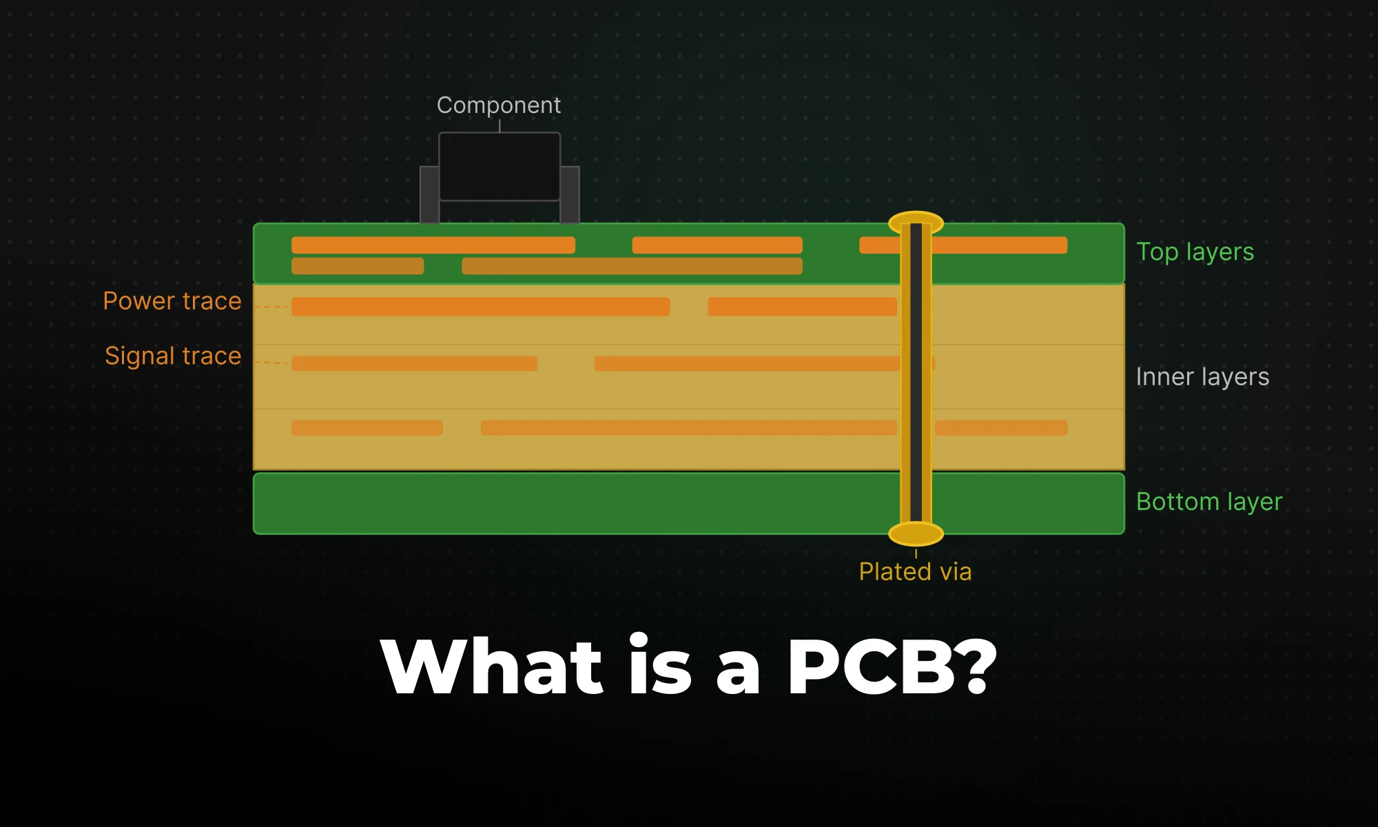
A Printed Circuit Board (PCB) is a rigid or flexible structure that mechanically supports and electrically connects electronic components using conductive pathways typically etched from copper. The PCB includes a laminated sandwich of conductive and insulating materials. During manufacturing, factories glue thin sheets of raw copper, known as copper foil, to a non-conductive base layer. They then chemically etch away the excess foil. This process leaves behind specific copper patterns: traces (which act as flat wires) and planes (which are large, solid areas of copper used to distribute power or ground).

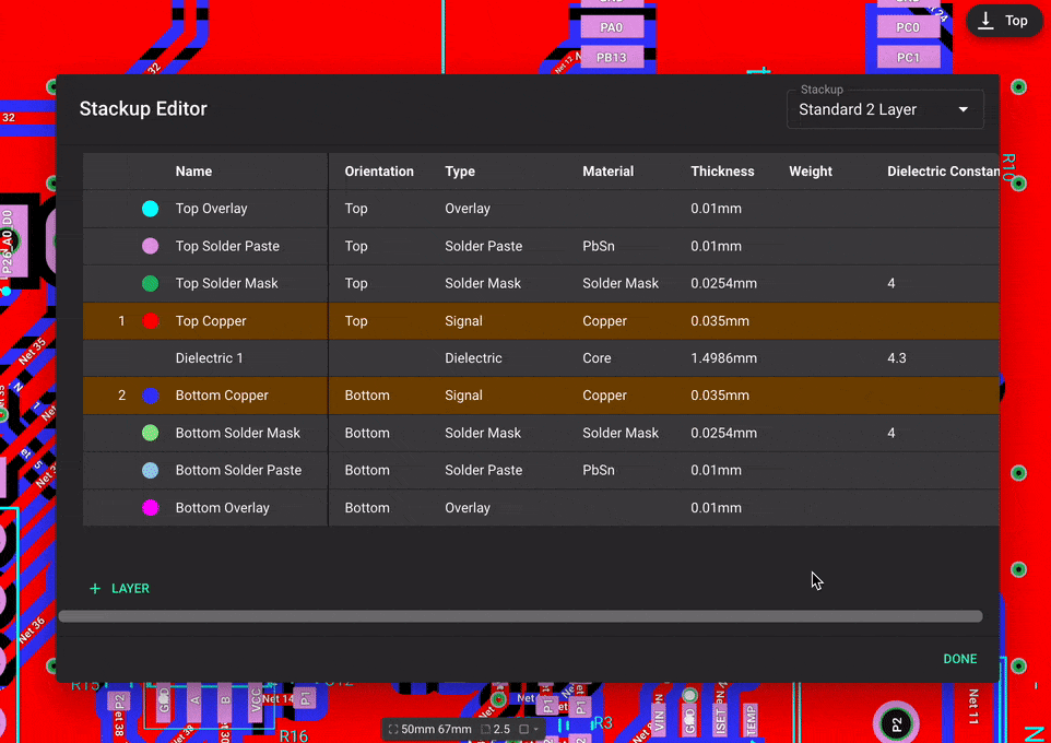
A standard rigid PCB has four primary layers:

Layer Description
Substrate (FR4) The structural core is usually FR4, which is a woven fiberglass cloth bonded with flame-retardant epoxy resin. FR4 dominates the industry. It captures over 40% of the global PCB material market because it is highly cost-effective and durable.
Copper Thin sheets of copper foil are laminated to one or both sides of the substrate, then chemically etched away during fabrication to leave only the desired electrical pathways.
Solder Mask A polymer coating applied over the copper. It gives boards their characteristic green color (though any color is possible), prevents accidental short circuits, and stops solder from bridging between closely-spaced traces during assembly.
Silkscreen An ink overlay used to print human-readable labels, part numbers, and component reference designators (like "R1" for a resistor) directly on the board surface.

How a Printed Circuit Board Works

Diagram of a PCB layer

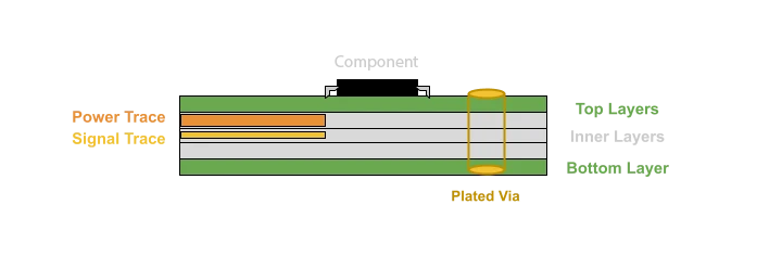
A printed circuit board acts as the electrical nervous system of a device. Instead of messy bundles of loose wires, the board uses flat copper lines to physically link the pins of different components together. Power and signals must travel across these physical pathways from power supplies to processors, and from sensors to memory, without degrading. Three structural features handle all this electrical traffic:

Traces are the etched copper pathways that carry current from one component to another. When routing these lines, designers manage two main variables: trace width and copper thickness. Trace width dictates how much current the path can safely handle. A power trace delivering 5 amps needs to be substantially wider than a simple data trace toggling at 3.3 volts. Copper thickness is measured in ounces (oz) per square foot, with 1 oz or 2 oz copper being common standards. If you size a power trace too narrow or use copper that is too thin, the electrical resistance increases. This generates excess heat and causes a voltage drop that can reset your processor mid-operation.

Pads are small, exposed copper areas, free of the green solder mask, where parts attach to the board. This is where you solder component leads (the long metal wire legs found on traditional through-hole parts) or surface-mount terminals (the flat metal contacts built onto the bodies of modern, low-profile chips). Every resistor, integrated circuit, and connector lands on a pad.

Vias solve the problem of routing signals across multiple layers. Vias are metal-lined drilled holes that enable electrical interconnections between conductive layers, essentially a copper-plated tunnel connecting a trace on layer 1 to a trace on layer 4, or any other layer combination.

Common PCB Components

A bare board with etched copper pathways does nothing on its own; it is essentially a blank canvas waiting for parts. It only becomes functional once you solder active and passive components onto those exposed pads. In manufacturing terminology, the bare board is the PCB; once populated with parts, it becomes a Printed Circuit Board Assembly (PCBA).

The components you choose dictate what the circuit does:

  • Resistors: Passive components that limit current flow, set specific voltage levels, and protect sensitive chips from overcurrent damage.
  • Inductors: Coil-like passive components that store energy in a magnetic field when electric current flows through them. They resist sudden changes in current, making them highly useful for filtering high-frequency noise and managing power in switching regulators.
  • Capacitors: Store and release electrical energy rapidly. Essential for filtering power-supply noise and stabilizing voltage delivery across the board.
  • Diodes: Semiconductor devices that allow current to flow in only one direction. They act as a one-way electrical valve, protecting your circuits from accidental reverse voltage.
  • Transistors: They act as electrically controlled switches or amplifiers, allowing you to turn digital signals on and off or boost analog waveforms.
  • Integrated Circuits (ICs): These silicon chips contain thousands or even millions of microscopic transistors packed into a single plastic or ceramic body. Instead of building a complex system out of individual discrete parts, engineers use ICs to perform heavy computational lifting. They function as microcontrollers that execute software code, memory chips that store user data, or operational amplifiers that process weak sensor inputs.
  • Connectors: Physical interfaces (USB ports, pin headers, edge connectors) that allow the board to exchange power and data with the outside world.

The PCB Design Process

Designing a printed circuit board follows a sequential engineering workflow. Whether a student is building a first prototype or a hardware startup is pushing a new consumer device to mass production, the core development cycle remains essentially the same.

  1. Schematic Capture: Everything starts with a schematic, a logical map showing how components connect to one another. This is the circuit's blueprint, independent of physical size or shape. See our schematic design guide for a full walkthrough.
  2. Component Selection: As you draw the schematic, you choose real, physical parts to correspond to each logical symbol. You decide on these specific components based on required electrical ratings. For example, ensuring a capacitor can handle the expected voltage or that a resistor has the correct wattage limit for your power needs.
    1. This generates a Bill of Materials (BOM) listing every component, its footprint dimensions, and its manufacturer part number.
  3. PCB Layout and Routing: Next, you import the schematic into Electronic Design Automation (EDA) software. Inside this layout tool, you arrange physical component footprints within a defined board outline and draw copper traces to connect them. Routing high-speed data lines or laying out power planes introduces complex signal integrity challenges, such as managing trace lengths and preventing electromagnetic interference. Modern platforms like Flux assist engineers directly in the browser by providing real-time design feedback and collaborative routing features, keeping the layout process moving quickly. Our PCB routing basics guide covers the fundamentals.
  4. Design Rule Checks (DRC): Before finalizing the layout, the EDA software runs an automated Design Rule Check against your manufacturer's specific fabrication constraints. Different industry standards establish various printed circuit board design rules regarding material selection, thermal management, and design for manufacturability (DFM). The most notable is IPC-2221, which determines the baseline clearance tables and electrical spacing guidelines that most DRC engines enforce.
  5. Gerber File Export and Fabrication: The Gerber format is an open, American Standard Code for Information Interchange (ASCII) vector format for PCB designs and is the de facto standard used by PCB industry software to describe board images: copper layers, solder mask, legend, drill data, and more. These files tell the factory exactly where to etch copper, drill holes, and apply solder paste. For a complete overview of this stage, see our electronics design workflow.

Types of Printed Circuit Boards

As circuits grow more complex, routing all connections on a single copper layer becomes geometrically impossible. The solution is adding layers. PCBs can be single-sided (one copper layer), double-sided (two copper layers on both sides of one substrate layer), or multi-layer (stacked layers of substrate with copper sandwiched between).

PCB Type Layer Count Typical Applications Cost & Complexity
Single-Layer 1 Basic power supplies, LED lighting, simple toys Lowest cost; severely restricted routing
Double-Layer 2 Industrial controls, audio equipment, basic instrumentation Moderate cost; traces can cross via top/bottom routing
Multilayer 4–32+ Smartphones, motherboards, high-speed networking gear High cost; required for ICs with high pin density and controlled impedance.

Rigid vs Flexible PCBs

Beyond layer count, boards split into rigid (standard FR4) and flexible (FPCB). Flexible PCBs are made from flexible materials like polyimide, allowing them to bend and fold to fit into compact and irregular spaces. They show up in folding smartphones, wearable devices, and camera hinges–anywhere a rigid board physically can't go.

Common Challenges in PCB Design

Three problems account for the majority of real-world board failures:

Signal interference (EMI/EMC) occurs when high-speed digital signals radiate electromagnetic fields that couple into adjacent traces, corrupting data. The fix isn't complicated in principle — proper trace spacing, ground planes, and controlled impedance routing — but it requires deliberate attention during layout. Many beginners overlook this entirely. They often only realize there is an issue when their first physical prototype mysteriously drops data or refuses to boot.

Power distribution is equally unforgiving. Modern microprocessors draw large bursts of current in microsecond windows. Traces that are too narrow create resistive voltage drops that cause processor resets or erratic behavior. The standard solution is to dedicate full internal layers of a multilayer board to power and ground — called power planes — rather than routing power as individual traces.

Manufacturing constraints (DFM) are where many first-time designers get burned. Drawing a functionally perfect schematic is only half the battle. Inside your layout software, you might sketch a 1-mil (0.0254mm) trace. That is an extremely thin line, roughly the width of a human hair, and standard factories simply cannot etch something that small. This gap between digital design and physical reality requires Design for Manufacturability (DFM) principles.

Industry standards like IPC-2221 dictate exactly how to handle material selection (such as picking a high-temperature substrate for a hot environment), thermal management (ensuring high-power chips can dissipate heat safely through the copper), and physical tolerances. Following these rules ensures your digital layout matches what a physical fabrication facility—often called a fab house—can actually build. Always check your specific manufacturer's capability guidelines before you route a single trace.

How Modern PCB Design Tools Help Engineers

Historically, PCB design meant expensive, desktop-bound EDA software. These legacy programs had steep learning curves that easily overwhelmed beginners. Furthermore, collaboration was practically non-existent. Teams passed zipped files of board layouts back and forth over email. This made it nearly impossible to work together on a class project or a startup prototype without creating confusing, conflicting versions.

The industry has moved on. Platforms like Flux bring the entire design workflow into a cloud-native, collaborative environment, making it much easier for new engineers to get started.

Flux: Collaborative, Browser-Based Electronics Design

Flux is a modern EDA platform built for the way hardware teams actually work today, in the browser, collaboratively, and with tight schematic-to-PCB integration.

  • Real-time co-editing Multiple designers can work on a schematic at the exact same time. If a student needs help with a circuit, an instructor or peer can open the exact same browser window to guide them. There are no locked files or confusing version mismatches.
  • Continuous DRC Design rule checks run constantly in the background as you draw your traces. For beginners who are still learning manufacturing constraints, this acts like a spell-checker for hardware. It flags spacing errors and trace width mistakes instantly, preventing you from spending money manufacturing a broken board.
  • AI-assisted component selection Reading 50-page technical datasheets is notoriously difficult for new hardware engineers. Built-in AI helps decode component specs and suggest the right parts. This means you spend more time actually designing and less time lost reading PDF files.
  • Tighter schematic-to-layout iteration As you update the logical schematic, the physical board layout updates dynamically. This tight feedback loop helps beginners visualize exactly how changing a wire connection directly affects the physical copper on the board.

For a hardware startup or a student building their first board, the difference between AI native PCB design software and a legacy desktop package isn't just convenience, it's the difference between shipping and stalling.

FAQs

What is a PCB used for?
A PCB is a physical board containing pre-made electrical copper traces and designated mounting slots for electronic components. While people often use the terms interchangeably, a bare board is technically just a PCB; once a factory solders the actual parts onto it, the hardware becomes a Printed Circuit Board Assembly (PCBA).
What is the difference between a PCB and a circuit?
A circuit is the logical path that electricity takes to perform a specific function. A circuit can exist purely as a digital schematic drawing, or it can take other physical forms, such as a temporary prototyping breadboard or manual point-to-point wiring. A PCB is the physical fiberglass-and-copper structure that physically implements that circuit.
What are the main components on a PCB?
The most common components are resistors (current control), capacitors (energy storage and noise filtering), integrated circuits (processing and memory), diodes (reverse-current protection), and connectors (external interfaces).
How are printed circuit boards manufactured?
The fabrication process starts by laminating thin copper foil onto an FR4 fiberglass substrate. Factories then use a chemical etching process to dissolve the excess copper, which leaves only your planned electrical traces behind. Next, they drill holes for vias and line them with metal to connect the inner layers, finishing the board by applying the protective green solder mask and readable silkscreen ink.
What software is used to design multilayer PCBs?
Engineers use Electronic Design Automation (EDA) tools. The industry is actively shifting from legacy desktop applications toward modern, cloud-based platforms like Flux that support real-time collaboration and continuous design rule checking.
|
March 21, 2026
Multilayer PCB Design: Best Practices for Circuit Board Layout

Multilayer PCB Design: Best Practices for Circuit Board Layout

Mastering multilayer PCB design is key for complex electronics. Use strategic stackup (Signal-Ground-Power-Signal), perpendicular routing, and solid ground/power planes to ensure signal integrity, reduce EMI, and support high-density components for applications like IoT and robotics.

Key Takeaways

  • Multilayer PCB design involves creating printed circuit boards with three or more copper layers, providing the routing space, EMI shielding, and component density needed for complex applications like IoT and robotics.
  • Carefully planning the layout of signal, ground, and power planes is critical for maintaining controlled impedance and providing uninterrupted signal return paths.
  • Applying proven PCB routing tips, such as routing adjacent signal layers perpendicularly and avoiding split planes, drastically reduces crosstalk and noise.
  • Cloud-native, AI-assisted platforms like Flux streamline multilayer PCB layout by enabling real-time team collaboration, automated design rule checks, and intelligent routing assistance.

What Is Multilayer PCB Design?

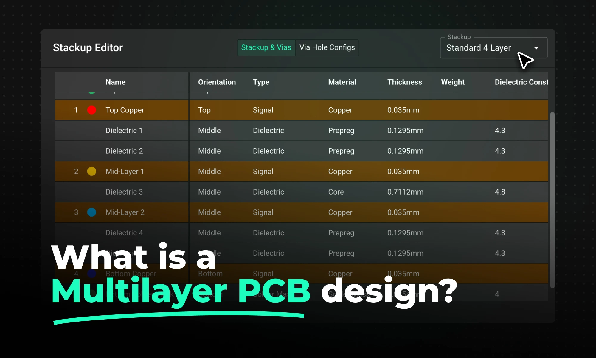
Multilayer PCB design is the design of boards with three or more copper layers separated by dielectric materials and laminated under heat and pressure, enabling internal routing of power and high-speed signals that single- and double-layer boards cannot provide for modern digital electronics.

Flux app showing how to easily select pre-definted default stackup configurations from top pcb manufacturers so you can get started quickly, also showing here is the ability to create your own custom pcb stackup configurations

In modern hardware, common layer counts include:

  • 4-layer boards: The standard starting point for boards featuring medium-density microcontrollers, typically structured as Signal / Ground / Power / Signal.
  • 6-layer boards: Used when more routing space is needed, or when separating high-speed digital signals from sensitive analog traces.
  • 8+ layer designs: Reserved for highly complex multilayer circuit board design, such as motherboards, advanced IoT gateways, or designs featuring high-pin-count Ball Grid Arrays (BGAs).

Why Multilayer PCBs Are Used in Modern Electronics?

The shift toward multilayer boards is driven by the physical constraints of modern components and the laws of physics at high frequencies. The primary benefits include:

  • Higher Component Density: High-density interconnect (HDI) packages and fine-pitch BGAs simply do not have enough physical space to route all escaping traces on a single surface layer. Internal layers provide the necessary real estate.
  • Improved PCB Signal Integrity: High-speed signals require a controlled impedance environment to prevent data-corrupting reflections. Internal routing adjacent to solid planes ensures predictable impedance.
  • Reduced Electromagnetic Interference (EMI): By burying noisy digital traces between solid copper ground or power planes, the planes act as a Faraday cage, absorbing stray radiation and preventing external noise from coupling into the board.
  • Better Power Distribution: Dedicated internal power and ground planes provide incredibly low-impedance paths for current, ensuring stable voltage delivery to power-hungry ICs while managing thermal dissipation.

Because of these advantages, multilayer architectures are mandatory for applications like IoT devices, robotics, and embedded systems.

How PCB Layer Stackup Affects Board Performance

The foundation of any high-performance board is its PCB layer stackup (the order and spacing of conductive copper and insulating dielectric layers in a PCB).  Stackup planning involves determining the order of signal layers, ground planes, and power planes, as well as the thickness and dielectric constant of the materials between them.

Proper multilayer PCB stackup design dictates how electromagnetic fields propagate through your board.

Common Multilayer Stackup Configurations

Layer Count Typical Arrangement Best Used For Key Advantages
4-Layer Top Signal, Ground Plane, Power Plane, Bottom Signal Standard microcontrollers, simple IoT sensors, and basic industrial controls. Cost-effective step up from 2-layer boards; provides basic EMI shielding and a solid return path for signals.
6-Layer Signal, Ground Plane, Inner Signal, Power Plane, Ground Plane, Signal Devices requiring dedicated high-speed routing, mixed-signal designs, and dense component placements. Safely buries sensitive high-speed traces internally; provides excellent impedance control and better EMI reduction.
8-Layer Signal, Ground, Signal, Ground/Power, Ground/Power, Signal, Ground, Signal Advanced motherboards, FPGA designs, high-pin-count BGAs, and RF applications. Maximum routing flexibility; isolates multiple power domains; superior electromagnetic compatibility (EMC) and thermal dissipation.

Key Stackup Considerations:

  • Signal Return Paths: High-frequency current typically follows the path of least inductance, which usually means directly beneath the signal trace on the nearest reference plane. A good PCB ground plane design ensures an uninterrupted return path.
  • Impedance Control: The distance between a signal layer and its reference plane dictates trace impedance (e.g., 50Ω single-ended).
  • EMI Reduction: Keep high-speed signal layers tightly coupled (physically close) to their respective ground planes to contain electromagnetic fields.

Best Multilayer PCB Routing Practices

Once your stackup is defined, the routing phase (process of connecting components with copper traces according to the schematic) begins. Executing a clean layout requires strict adherence to PCB routing best practices to avoid cross-coupling and timing errors.

  • Alternate Routing Directions: If you have adjacent signal layers (e.g., layers 3 and 4), route traces on one layer horizontally (X-axis) and the other vertically (Y-axis). This minimizes broadside coupling (crosstalk) between the layers.
  • Keep Traces Short: Especially for high-speed digital clocks and analog inputs. Shorter traces have less parasitic inductance and capacitance.
  • Separate Analog and Digital Signals: Never route noisy digital traces through an analog section of the board, and do not allow them to share the same return path space on the ground plane.
  • Differential Pair Routing: Route high-speed differential pairs (like USB or HDMI) perfectly parallel, matched in length, and completely symmetrical to ensure common-mode noise rejection (the ability to suppress noise appearing equally on both signal lines)..

Multilayer Routing Best Practices Checklist

  • Route adjacent signal layers in perpendicular directions.
  • Use dedicated, solid ground planes (avoid splitting them unless strictly necessary).
  • Keep high-speed signals short and route them on layers adjacent to a ground plane.
  • Minimize unnecessary vias, as each via introduces an impedance discontinuity.
  • Place decoupling capacitors on the top/bottom layers as close to the IC power pins as possible, dropping immediately to the internal power/ground planes.

Common Multilayer PCB Design Mistakes

Even experienced engineers can run into issues during complex layouts. Avoid these common pitfalls:

  • ⚠ Error
    Poor Layer Stackup Planning Routing high-speed signals on an inner layer that is sandwiched between two other signal layers (instead of planes) guarantees severe crosstalk and EMI issues.
  • ⚠ Error
    Improper Ground Plane Placement Creating a "split plane" (routing a void through the copper) and then routing a high-speed trace directly over that split. This destroys the return path, creating a massive loop antenna that radiates noise.
  • ⚠ Error
    Excessive Vias (The Swiss Cheese Effect) Placing too many vias too close together can create excessive holes in your internal ground plane that it effectively creates a continuous void, obstructing return currents.
  • ⚠ Error
    Signal Crosstalk from Poor Trace Spacing Failing to maintain the "3W Rule" (keeping the distance between trace centers at least three times the trace width) for high-speed nets.

How Modern PCB Tools Simplify Multilayer Design

Historically, multilayer PCB layout was performed on rigid, desktop-based EDA software that kept engineers siloed and required tedious manual constraint programming. Today, cloud-native, modern platforms like Flux are fundamentally shifting how hardware teams collaborate.

By bringing PCB design into the browser, modern tools offer a "multiplayer" environment where electrical engineers, layout designers, and mechanical engineers can view and edit the same board simultaneously.

Flux: Collaborative, Browser-Based Electronics Design

Flux is a modern EDA platform built for the way hardware teams actually work today, in the browser, collaboratively, and with tight schematic-to-PCB integration.

  • Real-time collaboration Multiple engineers can work on the same schematic at the same time, the same way you'd collaborate in a Google Doc. No more locked files or waiting your turn.
  • Browser-based access No installs, no license servers, no OS headaches. Open your design from any device and pick up where you left off.
  • Unified schematic and PCB environment The handoff from schematic to PCB layout happens inside the same platform, so nothing gets lost in translation between tools.
  • Automated design validation Built-in ERC catches connectivity issues, missing power references, and symbol errors in real time before they propagate into layout.
  • Version control and design history Every change is tracked, making it easy to review diffs, roll back to earlier revisions, and understand why a design decision was made.

Platforms like Flux also integrate AI directly into the workflow. Instead of manually cross-referencing datasheets for an 8-layer stackup or struggling to untangle a BGA breakout, hardware teams can leverage AI-assisted routing suggestions and an AI Copilot to check for PCB signal integrity risks, automate part selection, and run real-time design rule checks (DRCs). This drastically reduces the mental overhead of multilayer design, allowing engineers to iterate faster and catch errors before fabrication.

FAQs

What is multilayer PCB design?
Multilayer PCB design is the engineering process of creating a printed circuit board with three or more conductive copper layers. These layers are separated by dielectric material and allow for higher component density and complex internal routing.
How many layers should a PCB have?
The required number of layers depends entirely on circuit complexity and component density. Simple sensor nodes might only need 4 layers, while modern smartphones and computer motherboards often require 10, 12, or 16+ layers to route all signals and provide adequate ground shielding.
Why are ground planes important in multilayer PCBs?
Ground planes provide a low-impedance return path for electrical currents, which is vital for maintaining signal integrity. They also act as electromagnetic shields, preventing noise from coupling between adjacent signal layers or radiating off the board.
What are common multilayer PCB routing challenges?
Common challenges include managing impedance control across different layers, safely breaking out traces from high-density BGA packages, minimizing crosstalk between adjacent traces, and avoiding vias that disrupt internal ground planes.
What software is used to design multilayer PCBs?
Engineers use Electronic Design Automation (EDA) software to design multilayer PCBs. While legacy desktop tools have been the standard for decades, modern teams are increasingly moving to browser-based, AI-assisted, collaborative platforms like Flux to accelerate their design cycles.
|
March 19, 2026