March 26, 2026
High-Speed PCB Design: Layout Rules, Signal Integrity, and Routing Best Practices
Share

Key Takeaways
The most common misconception: a board only becomes "high-speed" once the system clock crosses some ultra-high threshold. That's wrong, and it's expensive to learn the hard way.
High-speed design becomes necessary when the signal's rise time approaches a critical threshold where transmission line effects become significant — specifically, when the signal rise time is less than four times the propagation delay. At that point, your copper traces stop acting as simple wires and start behaving as transmission lines. A transmission line is a distributed waveguide that directs high-frequency alternating currents; if you route or terminate it improperly, it functions as an accidental antenna, radiating electromagnetic interference across your entire board. Because of this, you must actively control characteristic impedance, mitigate reflections, and secure the return path.
Two practical rules of thumb help identify when you're in this territory:
Critically, it is the rise time of the device, not the clock frequency, that determines whether a design is high-speed. A fast device will create signal transitions that propagate far more aggressively than the clock rate alone suggests. Evaluate your design based on the parts, not the clock frequency.
Modern electronics are saturated with interfaces that easily exceed these thresholds. Typical high-speed signals engineers must route today include:
As signal speeds increase, physical board characteristics that were once negligible become dominant: traces behave as transmission lines where signals propagate as waves, and faster edge rates intensify electromagnetic coupling between adjacent traces.
Signal integrity is the measure of an electrical signal's quality as it travels from driver to receiver. When layout rules are ignored, high-speed edge rates trigger physical phenomena that compound rapidly.
Poor layout practices lead directly to four primary failure modes:
Return path management is where many engineers underestimate the physics of high-frequency loop inductance. At high frequencies, the return current takes the path of least inductance, which is directly underneath the forward current trace, because this path represents the smallest loop area. This is a fundamental departure from DC behavior, where current takes the path of least resistance.
Splits or holes in ground planes create uneven areas that increase impedance. These breaks force the return current to take detours, expanding loop areas and significantly increasing inductance and causing high-speed traces to act like antennas that radiate electromagnetic waves. This is the failure mode most engineers don't discover until they're staring at an EMC test failure.
Route high-frequency return currents along the path of least inductance. Implement solid ground planes under signal traces to minimize loop area and inductance. Avoid ground plane discontinuities such as slots, cutouts, or overlapping clearance holes to prevent current loops and noise.
High-speed design doesn't start during routing, it starts in the stackup manager. Get the stackup wrong, and no amount of careful trace routing will save you.
Your stackup dictates the distance between signal layers and their reference planes, which directly sets your characteristic impedance and EMI behavior. Every critical signal layer must be routed adjacent to a solid, unbroken ground or power plane. Routing two high-speed signal layers back-to-back without a reference plane between them creates "broadside coupling" — a severe crosstalk mechanism that's nearly impossible to fix after the fact.

A preferred method of PCB design is the multi-layer PCB, which embeds the signal trace between a power and a ground plane. For standard digital logic, engineers target 50Ω characteristic impedance for single-ended signals and 90Ω or 100Ω for differential pairs.
A high-frequency signal propagating through a long PCB trace is severely affected by a loss tangent of the dielectric material. A large loss tangent means higher dielectric absorption, and dielectric absorption increases attenuation at higher frequencies. Standard FR-4 is fine up to a few gigahertz. Beyond that, its loss tangent becomes the limiting factor.
*Megtron 6 Dk varies significantly with glass style: 1035 glass (65% resin) gives Dk 3.37, while 2116 glass (54% resin) gives Dk 3.61. Specify construction when quoting.
RO4350B provides a stable Dk of 3.48 from 500 MHz to over 40 GHz with minimal variation versus frequency, which makes it the go-to choice for RF and radar work where impedance consistency across a wide bandwidth is non-negotiable.
For most high-speed digital designs below 10 Gbps, high-performance FR-4 or mid-range specialized materials offer a good balance. For higher speeds or RF applications, premium materials become necessary despite their higher cost.
With the stackup locked, the routing phase demands strict adherence to geometric rules. Deviations that look harmless on screen show up immediately on a vector network analyzer (VNA) or oscilloscope.
Differential pair routing is the most common technique for high-speed serial interfaces. Because differential signals rely on equal and opposite voltages to cancel common-mode noise, both traces must be routed symmetrically, matched in length, and kept in parallel with consistent spacing throughout. Any asymmetry converts differential signals into common-mode noise, which your receiver cannot reject.
To prevent crosstalk between signals, apply the 3W Rule: the center-to-center spacing between adjacent traces should be at least three times the trace width. For 90°-bend corners, the geometry creates a localized increase in effective trace width, causing a drop in impedance and a reflection. Replace hard corners with 135° bends or smooth arcs throughout all high-speed runs.
Even experienced engineers make routing decisions that look clean on screen and fail in the lab. These are the specific layout errors worth memorizing before you spin your first high-speed prototype.
Routing over a plane gap is the most damaging single error. Empirical testing shows that traces crossing gaps in ground planes produce harmonics approximately 5 dBmV higher near the gap compared to traces over solid ground planes — and these gaps allow harmonics to appear even on unpowered traces, suggesting unintended coupling. The fix is simple: keep reference planes solid under every high-speed trace.
Other common pitfalls:
Traditional desktop EDA tools were designed for an era when schematic and layout were separate disciplines handled by separate people. A hardware engineer would finish the schematic, hand a netlist to a layout specialist, and wait — then review a PDF and email redlines back. For a DDR5 routing scheme with hundreds of length-matched signals, that workflow compounds every mistake.
Cloud-native platforms like Flux change the model. Collaborative PCB layout means entire engineering teams can view, edit, and troubleshoot a board simultaneously in the browser. This means no zipped project files, no version conflicts when a colleague needs to review a complex memory bus topology.
The more consequential shift is in design rule enforcement. Modern EDA platforms integrate automated design rule checks (DRC) that run continuously against your defined constraints — impedance targets, 3W spacing rules, differential pair length-matching tolerances — rather than as a batch step at the end. AI-assisted routing suggestions extend this further, flagging potential SI violations before they're committed to layout. The result is a tighter loop between constraint definition and physical implementation, which is exactly what high-speed design demands.


Flux's upgraded agent is more steerable, adaptive, and faster -- letting you change course mid-run, work in a single thread from idea to board, and ship hardware designs with less friction.

This Spring 2026 updates make hardware design faster end-to-end with a more capable, self-correcting AI agent, improved AI auto-layout that needs less cleanup, sourcing-aware design with real-time pricing and availability, and templates to start from.

With the latest release of Copilot it isn’t just smarter—it’s hands-on, placing components and applying bulk changes to your project instantly. But to get the most out of it, knowing how to craft the right prompt is key.
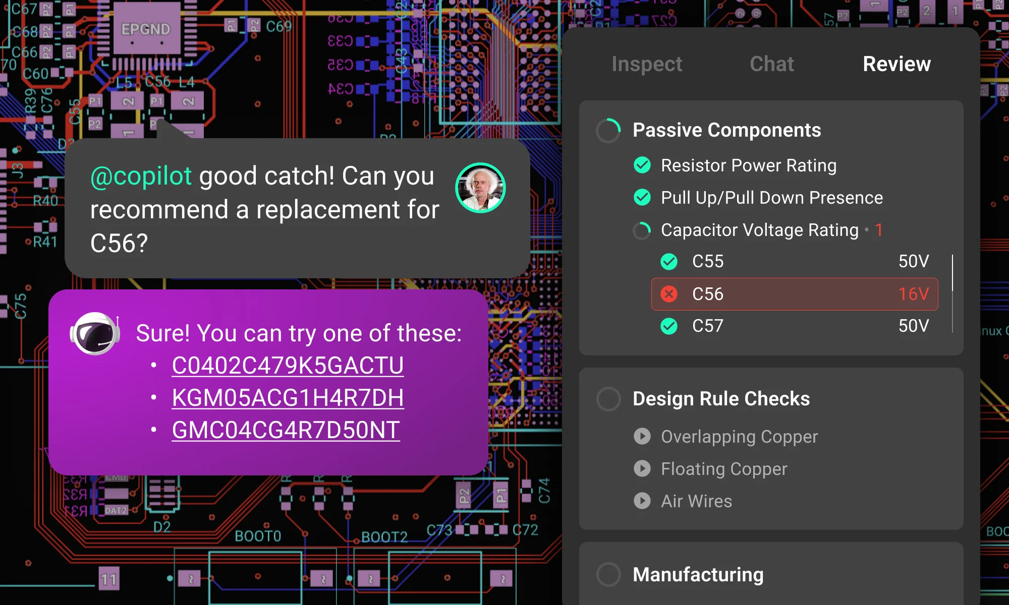
Creating a manufacturable, error-free PCB is never simple. Every engineer knows that missed details lead to production delays, costly revisions, and project setbacks. But what if you could have the power of a seasoned review team guiding you, 24/7?

How hardware teams apply Git-style version control to PCB design — tracking revisions, collaborating safely, and maintaining a complete design history.

A guide to flexible PCB design, covering materials, stackups, bend radius, and layout best practices for wearables, medical devices, and other compact electronics.

A beginner-friendly guide to reading PCB schematics, covering common symbols, nets, and how to follow signal flow through a circuit diagram.

Learn the key differences between analog and digital PCB design and how to manage mixed-signal layouts for better signal integrity.
