Files is a new top-level tab in Flux projects that centralizes all project documentation, including specs, uploaded assets, generated outputs, and project descriptions, in one place. This gives Flux full access to your project context, enabling better outputs, continuity across sessions, and easier team collaboration.
Describes Flux.ai's process of enabling 'noUncheckedIndexedAccess' in their TypeScript codebase. This setting enhances type safety by enforcing checks for possible 'undefined' values but introduces numerous type errors in a large codebase. To manage this, Flux.ai used heuristics and automation to suppress new errors with '!' and automate fixes using a provided script.
Flux.ai was started around 3 years ago in TypeScript with the default compiler settings. If we could go back in time, there is one setting we would surely change: noUncheckedIndexedAccess. By default, this setting is false. Many people believe it should be true.
What does noUncheckedIndexedAccess do? By default, TypeScript assumes any array element or object property you access dynamically actually exists:
In the example above, the function will throw an error if the string is empty, because str[0] returns undefined and doesn't have a toUpperCase function. TypeScript doesn't warn you about that, regardless of whether strict mode is enabled or not. This is a huge hole in type safety.
The flag noUncheckedIndexedAccess will plug that hole and force you to deal with the possible undefined:
So, why can't we just turn on noUncheckedIndexedAccess? You can, but in a large codebase like that of Flux.ai, you are likely to get thousands of type errors. We had 2761 errors across 373 files! For one speedy engineer converting one file every minute, it would have taken 6+ hours of mind-numbing work to convert all 373 files.
The solution we describe here is how to smoothly convert your codebase with some simple heuristics and automation.
According to Wikipedia, a heuristic technique
is any approach to problem solving or self-discovery that employs a practical method that is not guaranteed to be optimal, perfect, or rational, but is nevertheless sufficient for reaching an immediate, short-term goal or approximation.
That is definitely true here.
The goal was to get the codebase compiling with the new flag, not to fix any bugs. The fixing can come later.
To that end, we intentionally added type assertions ! to suppress all new type errors from undefined types without changing the runtime behavior of the code.
Expanding the scope of replacements to preceding lines allowed us then to automate more fixes with few false positives.
The full script we ran on our codebase is below. Note: it did not fix all the errors. It fixed around 2400 out of 2761 errors, leaving around 100 files for us to fix by hand.
Pro-tip: when experimenting with the replacers and precede, you can simply reset your changes with git reset --hard HEAD (assuming you are working in a git repo).
In this blog post, we explore how Flux.ai effectively uses Web Workers and ImmerJS to enhance data replication in our web-based EDA tool. We discuss our challenges with data transfer, our exploration of SharedArrayBuffer, and our ultimate solution using ImmerJS patches.
Web Workers are an established browser technology for running Javascript tasks in a background thread. They're the gold standard for executing long-running, CPU-intensive tasks in the browser. At Flux.ai, we successfully harnessed Web Workers, paired with ImmerJS patches, to minimize data transfer and deliver an ultra-fast user experience. This post will take you through our journey of using Web Workers and ImmerJS for data replication in our web-based EDA tool.
Flux.ai, an innovative web-based EDA tool, needs to compute the layout of thousands of electronic components simultaneously for its unique PCB layouting system. This process must adhere to user-defined rules. Our initial prototype revealed that layouting could take several seconds, leading us to explore the capabilities of Web Workers to parallelize this process and unblock the UI.
At bottom, the web worker API is extremely simple. A single method, postMessage, sends data to a web woker, and the same postMessage method is used to send data back to the main thread. We use a popular abstraction layer on top of postMessage, Comlink, developed several years ago by Google, that makes it possible to call one of your functions in a web worker as if it existed in the main thread. Newer, better or similar abstractions may exist. We did learn in using Comlink that it can easily blow up your JavaScript bundle size.
The trouble with using a web worker in a pure RPC style is that you most likely have a lot of data to pass through postMessage which is as slow as JSON.stringify, as a rule of thumb. This was definitely true in our case. We calculated that it would take 100ms at our desired level of scale just to transfer the layouting data each way, eating into the benefit of a parallel web worker.
A potential solution to the data transfer problem could be using SharedArrayBuffer, recommended for use with web workers. However, SharedArrayBuffer "represents a generic raw binary data buffer" meaning that a) it is of fixed size and b) it does not accept JS objects, strings, or other typical application data. Our investigations led us to conclude that the performance benefits were offset by the encoding and decoding costs in SharedArrayBuffer. One hope for the future is a Stage 3 ECMAScript proposal for growable ArrayBuffers.
We decided instead to populate our web worker with all the data on initial load of a Flux document (while the user is already waiting) and update it with changes as they happened. An added benefit of this approach is that the functions designed to run inside the web worker can also be run in the main thread with the flip of a global variable. You might want to do this for Jest tests, for example, which do not support web workers by default.
We got our changes in document data from ImmerJS, something we were already using as part of Redux Toolkit. Immer is an extremely popular library that enables copy-on-write for built-in data types via a Proxy. A lesser-known feature of Immer is Patches. The function produceWithPatches will return a sequence of patches that represent the changes to the original input.
We made a function that wraps produceWithPatches and assigns the patches back into the document for use downstream.
With the patches in hand, we could then complete our data flow from main thread to web worker and back again. The main thread calls the worker functions from middleware after every global state change. In Flux, we use redux-observable middleware.

In the code, the relevant functions look like this, assuming you are using Comlink.
The result of our use of Web Workers and ImmerJS patches was a significant reduction in workload on every document change and the ability for users to continue interacting with the application during a large re-layout - a priceless benefit in our web-based EDA tool.
For extra speed in our web worker, we forked the Immer applyPatches function. The original version was too slow for our needs. So, we adapted applyPatches to skip the draft step and mutate the target object in-place, resulting in a 10X speedup.
In conclusion, Web Workers and ImmerJS have proven to be powerful tools for efficient data replication in Javascript, particularly in the context of our web-based EDA tool, Flux.ai. They offer a potent combination for handling complex, CPU-intensive tasks, and improving user experience through faster data transfer and processing.
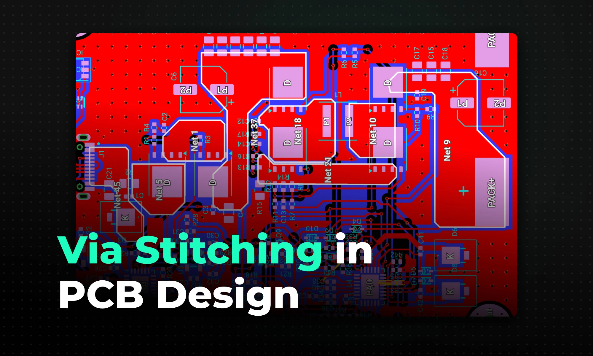
Via stitching connects large copper planes across multiple PCB layers with a dense array of vias, creating a three-dimensional ground structure that reduces impedance, shortens return current loops, suppresses EMI, and improves thermal dissipation.
Standard signal vias simply transfer a trace from one layer to another, and at low speeds, a single drilled hole does the job just fine. However, normal vias lose their utility when handling high-frequency signals and high-power components. Parasitic inductance spikes. Thermal energy builds up inside the substrate, and electromagnetic interference (EMI) radiates outward. Incorporating a via stitching pcb strategy mitigates these exact high-frequency issues. This technique connects large copper pours across multiple layers with a dense array of vias, transforming a flat copper plane into a three-dimensional ground structure. Done correctly, this structural shift reduces ground impedance, shortens return current loops, and protects signal integrity across the entire board.
Key Takeaways:
Via stitching is the placement of a periodic array of vias connecting copper planes across different layers in a multilayer PCB. Because inductors in parallel decrease total equivalent inductance, distributing multiple vias across a plane inherently lowers the connection's overall impedance. This parallel structure creates a low-impedance path for high-frequency currents, maintaining tight continuity where planes might otherwise split or transition.
Compared to traditional signal vias that route a discrete circuit trace from point A to point B, stitching vias operate with a different focus. While they certainly conduct electrical current, they usually tie large ground or power pours together rather than carrying specific data signals. This configuration ensures short return paths for surrounding traces and helps maintain a constant ground. Without that continuous return path, ground potential varies across the board, current loops physically expand, and noise follows.
In high-speed designs, discontinuities in reference planes can lead to increased loop inductance, which radiates energy as EMI. Via stitching addresses this by providing short return paths close to signal traces, minimizing field leakage.
A continuous low-impedance ground reference is non-negotiable for both signal integrity and regulatory compliance. Here is where via stitching delivers measurable results:
Knowing where to drop vias is just as important as knowing how many to use. Random scattering wastes board space and complicates routing. Target these specific locations during layout:
Avoid stitching planes too early in the design process. Fully stitched PCBs can hinder trace routing; always perform via stitching after completing signal and power routing.
Generic via placement will not meet the requirements of RF or high-speed designs. The spacing rule is mathematical, not intuitive.
A common guideline is to space vias at less than one-twentieth of the wavelength, the λ/20 rule, to ensure the structure blocks fields up to that frequency. Tighter spacing, such as λ/10, suits higher frequencies but increases via count.
Two concrete examples to put numbers to this:
One important note for digital designs: a 1 GHz digital data signal carries significant harmonic energy. The true operating bandwidth of these traces needs to be at least five times the fundamental frequency, or 5 GHz. For a good-quality digital signal, you need to pass at least the 5th harmonic of that signal. Size your stitching grid to the harmonic content, not just the clock rate.
These two techniques are frequently confused. Both use via arrays to improve board performance, but their geometry, placement, and purpose differ significantly.
An array of shielding vias can isolate sections of the design from the environment by creating a gap too small for the emitted wave to traverse. For this reason, via shielding is also known as via fencing.
Both arrays can exist simultaneously within a design, and layout designers need to understand the situations that warrant each rather than adding unnecessary cost with superfluous drilling. Via stitching is more forgiving than shielding; there is rarely a wrong opportunity for a short, low-impedance return path.
Poor implementation can degrade board performance rather than improve it. These are the errors that show up most often.
Too few vias. A sparse array fails to lower plane impedance meaningfully and won't capture high-frequency return currents. If vias are too far apart, they may fail to provide the necessary electrical or thermal benefits, compromising performance.
The "Swiss cheese" ground plane. The opposite problem is equally damaging. If vias are placed too close together, they can weaken the board structure, increase manufacturing costs, and cause issues like drill breakage during production. Clustering vias too tightly carves up the ground plane, reduces copper volume, and forces return currents to navigate around via holes — the exact problem you were trying to solve.
Additional mistakes to avoid:
Manually dropping hundreds of vias into a ground plane is tedious and error-prone. Modern EDA tools handle the repetitive work so you can focus on the design decisions that actually require judgment.
Flux handles layout automation through object-specific rules and intelligent copper structures. By applying a Fill Stitching Density rule directly to your ground net, Flux automatically generates a precise grid of stitching vias wherever those copper planes overlap. If you need a strict 2.5 mm by 1.5 mm staggered grid, the software calculates and places the array instantly.
For custom copper shapes, the Smart Polygons feature takes this a step further. When you extend a Smart Polygon across multiple layers, Flux automatically applies via stitching to bind the structure electrically. This eliminates the need to calculate custom via arrays for irregularly shaped RF sections or thermal pours.
While these rules manage the bulk copper connections, the Smart Vias feature independently automates the selection and configuration of blind, buried, and micro vias for standard trace routing.
Beyond placement, Flux provides:
Now that you understand the mechanics of via stitching pcb designs, it's time to put these principles into practice. Start your next layout with confidence and easily manage via arrays, thermal constraints, and low-impedance return paths using intelligent automation. Try Flux for free today to build faster, cleaner boards with built-in design rule checks and an AI copilot by your side.
Signal integrity in PCB design is the measure of how accurately an electrical signal travels from a driver to a receiver without distortion — with most problems stemming from impedance mismatches, poor return paths, and crosstalk, which lead to data errors and EMI issues.
Signal integrity (SI) measures the quality of an electrical signal as it travels from a transmitting source to a receiving load. In PCB design for signal integrity, this means ensuring signals arrive without distortion or timing errors. In an ideal case, a digital signal reaches the receiver unchanged, but in reality, PCB traces and materials introduce delay, attenuation, reflections, and noise.
As switching speeds increase and edge rates shrink to sub-nanosecond levels, even “low-frequency” signals behave like high-frequency ones. For example, a 100 MHz clock with a 500 ps rise time contains frequency components well into the GHz range. That’s where PCB parasitics start winning.
For circuit boards with serial or parallel buses, there is a minimum speed threshold at which a designer should consider transmission line effects. A widely accepted rule of thumb is that this threshold occurs when the trace length exceeds 1/10th of the signal's wavelength. For digital signals, the critical length is also commonly stated in terms of rise time: a trace whose propagation delay exceeds one-tenth of the signal's rise time should be treated as a transmission line.
Poor SI directly degrades system reliability. When signals distort, the receiver struggles to determine whether a voltage level represents a logic high or low. That ambiguity becomes data corruption, false switching, and timing violations.
Signal degradation also introduces timing variations known as jitter. In high-speed serial links, jitter shrinks the data eye — the valid window in which the receiver can sample a bit cleanly. If the eye closes completely, the system experiences a high bit error rate (BER). For example, for USB 3.0, the specification mandates a BER of 10⁻¹², which requires transmitting nearly 3×10¹² bits without error to confirm compliance at 95% statistical confidence. Miss that target and you're either failing compliance testing or dropping connections in the field.
The interfaces most sensitive to signal integrity failures include:
When a signal travels down a transmission line, any change in its environment disrupts propagation. The most frequent problem is reflections from an impedance mismatch. If a 50-ohm trace necks down to pass between two via pads, the impedance changes at that point. A portion of the signal's energy reflects back toward the driver, collides with subsequent transitions, and causes voltage ringing at the receiver.
Crosstalk is equally pervasive. Capacitive coupling transfers voltage spikes between parallel traces; inductive coupling transfers current spikes. Either mechanism injects noise into adjacent nets that can trigger false logic transitions if the amplitude exceeds the receiver's noise margin.
High-frequency signals also suffer from two distinct attenuation mechanisms:
Characteristic impedance is the ratio of voltage to current a signal experiences as it travels down a transmission line. Maintaining a constant value requires uniform trace width, uniform copper thickness, and a consistent distance to a reference plane. Change any of those parameters mid-route and you've created a reflection point.
Return paths are just as important as the forward trace. At low frequencies (below roughly 100 kHz), return current takes the path of least resistance. Above roughly 10 MHz, it takes the path of least inductance, which means it flows directly beneath the forward trace when a solid reference plane is present. That tight coupling minimizes loop area and suppresses EMI. Disrupt the plane and the return current detours, the loop expands, and your board starts radiating.
Termination absorbs signal energy at the end of a trace to prevent reflections. A series resistor at the driver (source termination) or a shunt resistor to ground at the receiver (parallel termination) matching the trace's characteristic impedance dissipates the energy rather than reflecting it.
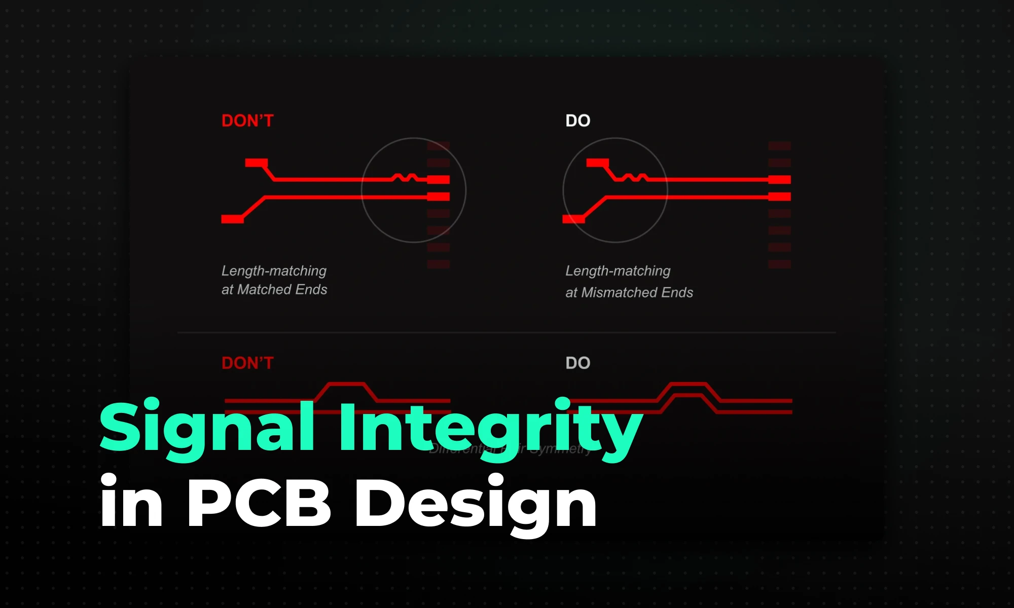
Differential signaling is the standard approach for any interface above a few hundred megabits per second. A differential pair carries a signal and its inverse on two tightly coupled traces. The receiver measures the voltage difference between them, so common-mode noise that couples equally onto both traces cancels out mathematically. That's why USB, PCIe, HDMI, and virtually every other high-speed interface uses differential pairs.
Every geometric decision you make on the canvas has an electrical consequence. Trace length directly sets DC resistance and dielectric loss. This means longer traces attenuate high-frequency harmonics faster, rounding the edges of a digital square wave into something that looks increasingly analog. That's not a simulation artifact; it's physics.
The layer stackup may be the single most important SI variable in your design. The distance from a signal layer to its reference plane determines characteristic impedance and return current loop size. A stackup that buries high-speed signals far from a reference plane guarantees excessive crosstalk and radiation. These problems are expensive to fix after fabrication.
Vias are a specific hazard. The parasitic inductance of a via can be estimated using the empirical formula L = 5.08h[ln(4h/d) + 1], where h is the via length and d is the diameter of the center hole. The length of the via has the greatest influence on inductance, while diameter matters far less. At multi-GHz frequencies, the unused portion of a through-hole via barrel acts as a resonant stub, severely attenuating specific frequencies. Back-drilling, removing the stub by drilling out the unused barrel, is the standard fix for high-speed SerDes interfaces like PCIe Gen 4 and above.
The goal is simple: give electromagnetic fields an uninterrupted, controlled environment to propagate through. Fixing SI problems after a board fails compliance testing means a respin. Here's how to get it right during layout.
Calculate the exact trace width and spacing needed for your target impedance before routing begins. Calculating the dielectric constant, width, and trace thickness determines the trace width for controlled impedance routing. Since changing the board stackup or fabrication materials alters these calculations, the layer configuration must be locked before layout starts. Tell your fabricator which nets require controlled impedance so they can adjust the etch process to hit your target within ±10%.
When a signal must change layers, place a ground return via directly adjacent to the signal via. Adding ground vias within 20 mils of each signal via, and between and around differential pairs, provides a low-inductance return path and maintains impedance through the layer transition.
Routing a high-speed trace over a split or gap in the ground plane is the single most destructive layout error. When the return current flowing beneath the trace hits a gap, it must detour around the split. That detour creates a large current loop, and large loops radiate. The board effectively becomes a broadcast antenna for whatever frequency the signal carries.
Ignoring impedance control until late in the design is nearly as damaging. Routing high-speed signals at whatever default trace width the tool suggests (often 8–10 mils) is a near-guarantee of impedance mismatches. Impedance targets must be defined, calculated, and enforced in your design rules before a single high-speed net is routed.
Two more mistakes that consistently cause failures:
Traditional SI workflows follow a painful pattern: finish the layout, export the files, import into a standalone simulation tool, discover the routing mistakes, and go back to square one. Engineers often find problems weeks after they are introduced.
Flux addresses this with an automatic controlled impedance calculation tool that calculates the required impedance for a board design without manual input — a designer configures their high-speed signal to a specific protocol, and the tool calculates and implements the controlled impedance values. Flux also includes automated design rule checks, supply chain monitoring, and manufacturability validation — all within the browser, without installing anything.
Flux is designed with the future of hardware design in mind, with AI integration, real-time collaboration, and workflows that scale for both solo designers and large hardware teams. When the tool enforces impedance constraints during routing rather than flagging violations after the fact, you catch errors before they require a prototype respin. That shift, from post-design audit to in-design enforcement, is where modern tooling earns its keep.
Now that you understand the core concepts behind signal integrity pcb design, you're ready to put these best practices into action. Don't let impedance mismatches or poor return paths derail your next high-speed project or push you into an expensive prototype re-spin. Try Flux today to access automated impedance control, real-time DRCs, and a modern, collaborative layout environment that helps you build reliable hardware faster.
The most common PCB design mistakes stem from poor component placement, incorrect trace routing, and weak grounding — all of which degrade signal integrity and can lead to costly manufacturing failures or board re-spins.
A printed circuit board (PCB) that looks complete in your EDA tool can still fail in three distinct ways:
According to BCC Research, the global PCB market was projected to grow from $70.9 billion in 2024 to $92.4 billion by 2029. This means design teams face mounting pressure to get boards right on the first pass as product complexity scales.
The most expensive failures aren't always dramatic. Intermittent signal corruption, thermal throttling under load, or a batch of boards that fail incoming inspection are all common outcomes of mistakes that were entirely preventable at the design stage. A trace width violation corrected in software costs nothing. The same violation found after a fabrication run can scrap an entire batch.
The five categories below represent PCB design mistakes that consistently appear in real boards, with concrete examples and corrective actions you can apply directly in your layout.
Placement is the foundation of every routing decision that follows. Early placement sets the physics of your board; where current flows, where heat concentrates, how connectors meet the real world. Once component placement is locked in, everything else becomes more expensive to change: routing gets tighter, layer counts creep up, and mechanical constraints turn into late-stage compromises.
Thermal interference: IPC-2221 offers recommendations on where to place components to achieve the best thermal performance, which involves keeping heat-generating components away from sensitive ones and ensuring components have enough thermal relief to avoid thermal stress. Position heat-generating components like power transistors or regulators away from sensitive parts to prevent overheating, and maintain at least 0.5 inches of clearance around high-power components as a practical starting point, though your specific layout and enclosure may require more.
Long or convoluted signal paths: For designs involving high-speed signals operating above 100 MHz, component placement directly impacts signal integrity — place sensitive components like microcontrollers or RF modules close to their associated circuitry to minimize trace lengths and routing complexity.
Assembly and depanelization risk: For large-scale production, PCBs are often assembled in panels. During SMT component placement, ensure that components near panel edges have extra clearance – at least 5 mm, to account for depanelization processes like routing or scoring. This prevents damage to components during separation.
Placement best practices that prevent all three failure modes:
Trace routing mistakes range from obvious to subtle. All of them degrade signal quality, generate EMI, or risk thermal failure under load. Getting trace routing right means addressing three key areas: trace geometry (angles), width control, and effective via usage.
The conventional guidance to avoid 90° corners and use 45° bends is widely taught, but the underlying reason matters. A 90° bend introduces excess copper compared to a straight trace. This additional copper increases localized capacitance, which can cause small signal reflections. How big an impact a corner has depends on the rise time of the incident signal and how much excess capacitance is in the corner.
If we use a condition of a return loss below -15 dB as insignificant, a 20.5 mil wide trace is transparent below 25 GHz. For the vast majority of digital designs, 90° corners are not a signal integrity crisis. The practical reasons to prefer 45° bends are real but more modest: they reduce routing length, lower the risk of acid trap formation during etching, and are flagged by peer reviewers as poor practice. For consumer electronics and general hardware, 45° corners are a safe, high-performing default. In RF and microwave designs, avoid them entirely.
A common mistake is using the same trace width across an entire design regardless of the current load. Trace width determines how much current a PCB track can carry without overheating, and IPC-2221 includes charts and formulas to calculate the appropriate width based on current, copper thickness, and temperature rise.
For a quick approximation with 1 oz copper on an external layer, 1 amp requires roughly 10 mils of trace width at a 10°C temperature rise. That's a useful starting point, but it's only an approximation. For a 1 amp current with a 10°C temperature rise, IPC-2221 may call for a trace width of about 20 mils on 1 oz copper, depending on the calculation method and temperature rise budget used. Always use an IPC-2221 calculator with your actual parameters rather than relying on the "10 mils per amp" shorthand for power traces. Internal traces are sandwiched between insulating layers of FR4 and cannot dissipate heat to the air like external traces can. As a result, internal traces need to be roughly twice as wide as external traces to carry the same current safely.
For high-speed signals, width is governed by impedance targets, not current. Use a controlled-impedance calculator for clocks, DDR, USB, and similar nets.
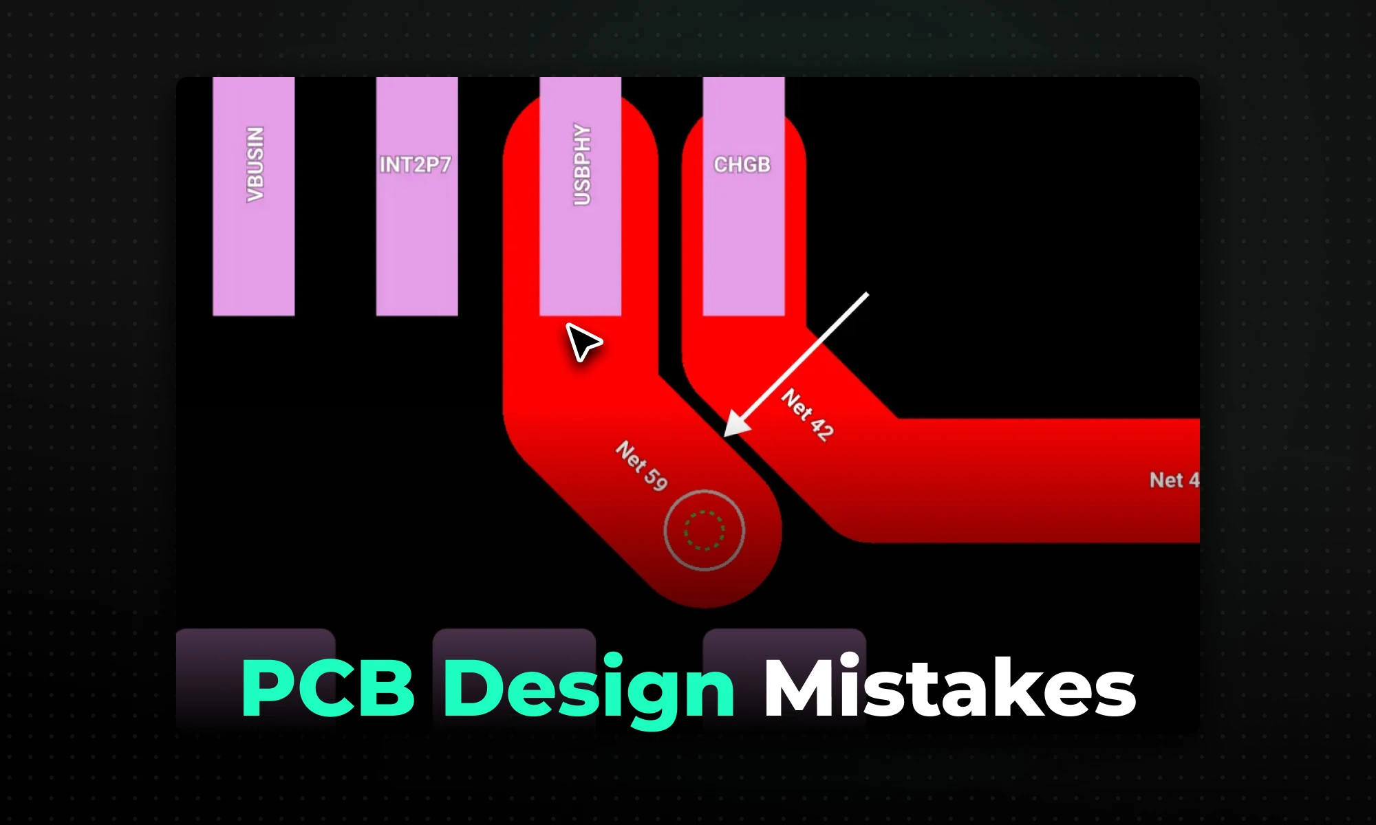
Vias are speed bumps for high-speed signals; they introduce parasitic capacitance and inductance. Minimize via count; ideally, high-speed signals should stay on one layer. Each layer transition also breaks the return path unless you place a stitching via nearby.
Routing Best Practices Checklist
Every signal that travels through a trace has a return current that flows back to its source. This is simple physics, but in practice it's one of the most misunderstood aspects of PCB layout, and the source of a disproportionate share of EMI failures.
Return current doesn't take the shortest physical route. It takes the path of least impedance, which means following directly under the signal trace when a solid ground plane is present. This tight coupling between signal and return minimizes loop area, and loop area is what determines both radiated emissions and susceptibility to external noise.
Grounding best practices:
Stable power delivery is as important as the signal routing above it. When an active device switches states, it draws a sudden transient current. That transient causes a voltage drop across the connecting traces due to their inherent impedance — and if there's no local energy reservoir to supply it, the voltage rail sags.
The consequences are concrete: a microcontroller can enter brownout mode, and any ADC conversion on an unstable analog supply is essentially useless. Use two capacitor values per power pin to cover the frequency spectrum:
Place decoupling capacitors within 1–2 mm of the power pins of an IC to effectively filter noise. A 0.1 µF capacitor placed too far away may fail to stabilize voltage fluctuations during high-frequency operation.
Routing discipline matters here too: route power from the source to the capacitor first, then from the capacitor to the IC power pin. Branching directly to the IC and then to the capacitor defeats the purpose, the transient current bypasses the capacitor entirely.
Design rule violations don't fail visually in your EDA tool. The board looks complete. The ratsnest clears. Files generate. Then the fabricator rejects the job, or worse, the boards come back and fail in ways that take weeks to diagnose.
IPC-2221 defines the generic design requirements for organic printed circuit boards, serving as the foundational guideline for building reliable circuit boards. DRC is the automated mechanism for enforcing those requirements during layout.
The most important DRC habit most beginners skip: don't use default software rules. IPC-2221 specifies the recommended component clearance for automatic placement machines — you'll want to set this value in the software and have it automatically detect violations when the rule is breached. Always load your fabricator's specific rule file before layout begins.
Run DRC continuously, not just at the end. Real-time DRC catches violations as you route; a full batch DRC run immediately before Gerber generation catches anything that slipped through.
Use this checklist before sending fabrication files.
Component Placement
Trace Routing
Grounding
Power Distribution
Design Rules
The mistakes described in this article aren't new. The tools for catching them earlier, however, have improved significantly — and the shift is meaningful: from reactive (catching errors after layout is complete) to continuous (flagging violations as you design).
Noteworthy features available in modern tools include live design rule check (DRC), live simulation tools, and generic component design options. Tools like Altium Designer, KiCad, and Cadence OrCAD X all offer real-time DRC, with varying degrees of integration with simulation and review workflows. Run checks frequently as you design rather than saving DRC for the end.
Collaborative review is equally important. A second set of eyes, whether a senior designer or a tool-assisted layout audit, consistently catches errors that the original designer is blind to after hours of staring at the same layout.
Flux is built to feel like a desktop-class tool without installs: large, multi-layer designs run smoothly in a modern browser, with real-time collaboration built in. Flux includes automated design rule checks, supply chain monitoring, and manufacturability validation. What sets Flux's AI design reviews apart is their ability to leverage the project's context and detailed data — part datasheets, application notes, and design constraints — to provide deep, actionable insights. Unlike simple DRCs limited to binary pass/fail results, these checks are context-aware and interpretive, giving you insights into whether a design meets best practices, maintains safety margins, and is optimized for production.
For teams working across locations or discipline boundaries (firmware engineers reviewing signal paths, for example) the collaborative model eliminates the revision-by-email cycle that delays error discovery until late in the process.
Now that you understand how to identify and avoid the most common pcb design mistakes, the next step is building these best practices into your regular workflow. Instead of waiting for a final review to catch errors, you can start your next design with a tool engineered to help you succeed on the first pass. Try Flux today to get real-time DRC feedback, AI Copilot design reviews, and seamless collaboration built directly into your browser.
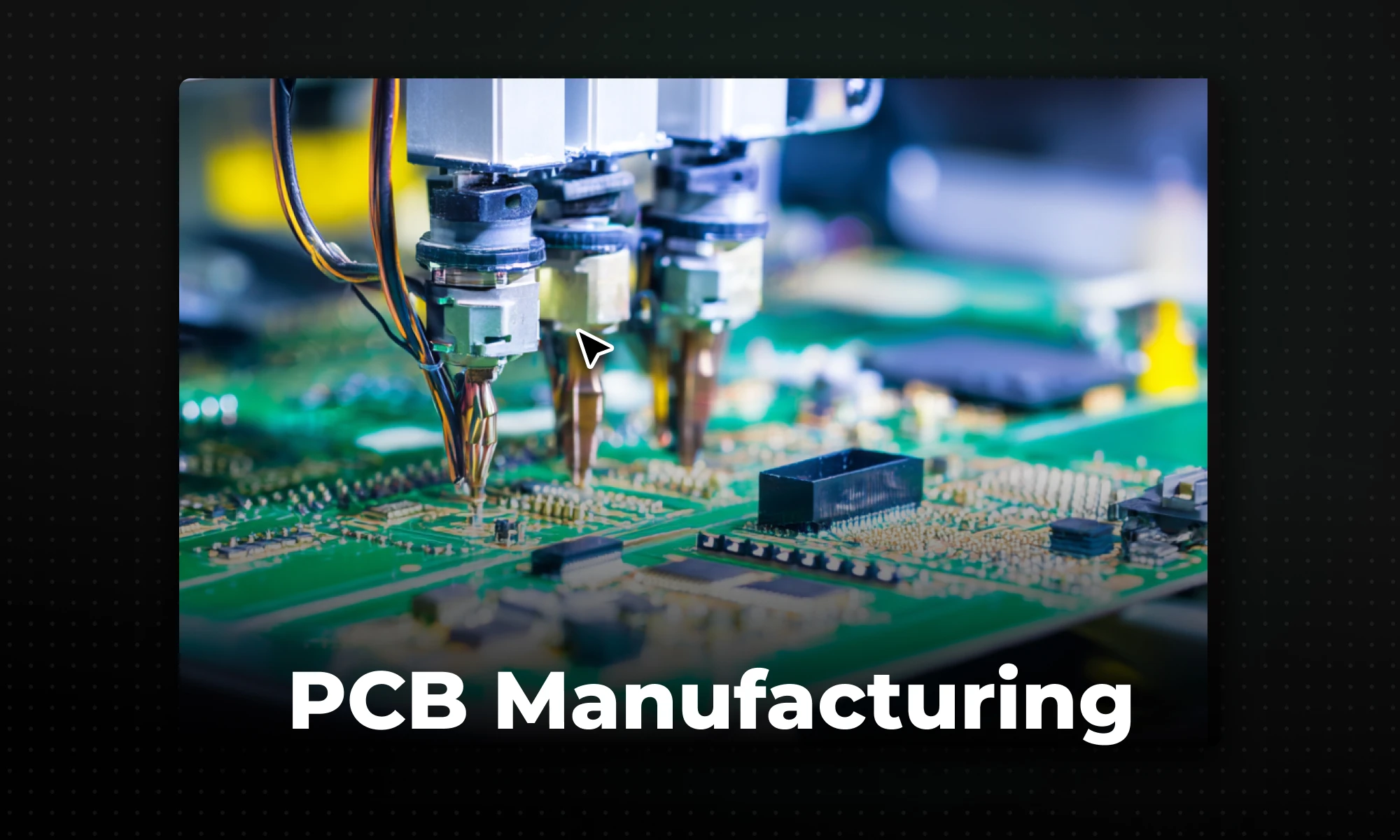
PCB manufacturing is a two-part process — fabrication builds the bare board through chemical etching and precision drilling, while assembly uses robotic pick-and-place machines and reflow soldering to attach the electronic components.
Transforming an idea into a physical, functioning electronic device can feel like magic. In reality, it is the result of a precise and standardized industrial workflow. Understanding how printed circuit boards are manufactured is crucial for any hardware engineer or electronics student.
This guide breaks down the entire PCB manufacturing process into simple, easy-to-understand stages. Whether you are curious about how the bare board is built or how microscopic components are attached, this step-by-step breakdown will demystify the journey from design to reality.
The PCB manufacturing process is the complete cycle of turning a digital circuit design into a physical, functional circuit board. It bridges the gap between software-based engineering and real-world hardware.
When a designer finishes routing a board on their computer, they export a set of manufacturing files. The manufacturer then uses these files to guide machinery, chemical baths, and robotic arms to construct the board. The circuit board manufacturing process is strictly controlled to ensure every board functions exactly as designed.
The entire PCB production process is generally divided into two distinct halves: making the bare board, and attaching the parts to it.
For beginners, the terms "fabrication" and "assembly" are often used interchangeably. However, understanding the difference between PCB fabrication vs assembly is critical, as they are two completely different manufacturing stages (and are sometimes even done by different specialized companies).
The pcb fabrication steps require a mix of photolithography, chemistry, and precision drilling. Here is how the bare board is made:
1. Design Output (Gerber Files)
The process begins when the designer exports their layout into an industry-standard format, typically Gerber files or ODB++. These files act as the blueprints for the manufacturer's machines, detailing exactly where every copper trace, drill hole, and label should go.
2. Layer Imaging
The manufacturer starts with a piece of core material (usually FR4 fiberglass) coated in solid copper. The board is covered with a light-sensitive film called photoresist. Using UV light and the Gerber files, the exact circuit pattern is "printed" onto the photoresist, hardening the areas where copper needs to stay.
3. Etching Copper
The board is submerged in a chemical bath. The hardened photoresist protects the desired copper pathways, while the chemicals dissolve and wash away all the exposed, unwanted copper. Once the photoresist is removed, only the intended copper circuit remains. (Note: For multilayer PCB design, this process is repeated for inner layers, which are then pressed and bonded together under high heat).
4. Drilling Holes
Precision computer-controlled drills create holes through the board. These holes serve two purposes: mounting holes for securing the board, and "vias," which are tiny holes that allow electrical signals to travel between different layers of the board.
5. Plating
The drilled board undergoes a chemical process that deposits a thin layer of copper over the entire surface and, most importantly, inside the walls of the drilled holes. This connects the different layers of the board together electrically.
6. Solder Mask Application
The board is coated with a liquid photoimageable solder mask—this is what gives a PCB its iconic green color. The mask protects the copper traces from oxidation and prevents solder from accidentally bridging closely spaced traces during assembly. Openings are left in the mask only where components will be soldered.
7. Silkscreen
Finally, a printer applies ink to the board to add human-readable information. This includes component designators (like "R1" or "C2"), company logos, pin 1 indicators, and warning labels.
Once the bare boards are fabricated and tested, they move to the PCB assembly process. This turns the bare board into a functioning electronic device.
1. Solder Paste Application
A stainless steel stencil is placed over the bare board. A machine wipes a squeegee across the stencil, pressing a specialized solder paste (a mixture of tiny solder balls and flux) through the holes. This ensures solder paste is applied exactly and only onto the exposed copper pads where components will sit.
2. Pick-and-Place
The board moves onto a conveyor belt into a robotic pick-and-place machine. Using vacuum nozzles and optical alignment, this incredibly fast robot picks up tiny components from reels or trays and places them perfectly onto the wet solder paste.
3. Reflow Soldering
The populated board is sent through a long reflow oven. The board passes through several temperature zones that gradually heat the board, melt the solder paste to form solid electrical connections, and then cool it down at a controlled rate to prevent thermal shock.
4. Inspection and Testing
After soldering, the board must be inspected. Automated Optical Inspection (AOI) machines use cameras to check for missing components or bad solder joints. For complex boards with hidden connections, X-ray inspection is used. Finally, the board undergoes functional testing to ensure it operates exactly as intended.
Despite automation, circuit board production is complex, and physical realities can cause issues. Common challenges include:
A board's success on the manufacturing floor is dictated weeks earlier during the design phase. Poor design choices inevitably lead to production issues.
For example, placing components too close to the edge of the board can cause them to crack during assembly. Routing traces too close together can lead to etching failures. This is why following a PCB design for manufacturability guide (DFM) is so critical. DFM ensures that the engineer's digital layout respects the physical tolerances of the manufacturer's machines. By utilizing smart PCB routing techniques, designers can ensure their boards are built reliably, cheaply, and on time.
Historically, preparing a design for manufacturing involved a disconnected, desktop-based workflow full of manual checks and zip files. Today, modern platforms are bridging the gap between design and production.
Flux provides a collaborative, browser-based environment that aligns perfectly with a modern design-to-manufacturing workflow. Because Flux runs in the cloud, teams can collaborate in real-time, catching potential manufacturing errors before they happen. With built-in, real-time design rule checks (DRC) and easy exporting of manufacturing files, Flux ensures that when you are ready to hit "manufacture," your design is fully prepared for the fabrication and assembly stages without the traditional friction.