June 24, 2026
How to Use Via Stitching in PCB Design
Share

Standard signal vias simply transfer a trace from one layer to another, and at low speeds, a single drilled hole does the job just fine. However, normal vias lose their utility when handling high-frequency signals and high-power components. Parasitic inductance spikes. Thermal energy builds up inside the substrate, and electromagnetic interference (EMI) radiates outward. Incorporating a via stitching PCB strategy mitigates these exact high-frequency issues. This technique connects large copper pours across multiple layers with a dense array of vias, transforming a flat copper plane into a three-dimensional ground structure. Done correctly, this structural shift reduces ground impedance, shortens return current loops, and protects signal integrity across the entire board.
Via stitching is the placement of a periodic array of vias connecting copper planes across different layers in a multilayer PCB. Because inductors in parallel decrease total equivalent inductance, distributing multiple vias across a plane inherently lowers the connection's overall impedance. This parallel structure creates a low-impedance path for high-frequency currents, maintaining tight continuity where planes might otherwise split or transition.
Compared to traditional signal vias that route a discrete circuit trace from point A to point B, stitching vias operate with a different focus. While they certainly conduct electrical current, they usually tie large ground or power pours together rather than carrying specific data signals. This configuration ensures short return paths for surrounding traces and helps maintain a constant ground. Without that continuous return path, ground potential varies across the board, current loops physically expand, and noise follows.
In high-speed designs, discontinuities in reference planes can lead to increased loop inductance, which radiates energy as EMI. Via stitching addresses this by providing short return paths close to signal traces, minimizing field leakage.
A continuous low-impedance ground reference is non-negotiable for both signal integrity and regulatory compliance. Here is where via stitching delivers measurable results:
Knowing where to drop vias is just as important as knowing how many to use. Random scattering wastes board space and complicates routing. Target these specific locations during layout:
Avoid stitching planes too early in the design process. Fully stitched PCBs can hinder trace routing; always perform via stitching after completing signal and power routing.
Generic via placement will not meet the requirements of RF or high-speed designs. The spacing rule is mathematical, not intuitive.
A common guideline is to space vias at less than one-twentieth of the wavelength, the λ/20 rule, to ensure the structure blocks fields up to that frequency. Tighter spacing, such as λ/10, suits higher frequencies but increases via count.
Two concrete examples to put numbers to this:
One important note for digital designs: a 1 GHz digital data signal carries significant harmonic energy. The true operating bandwidth of these traces needs to be at least five times the fundamental frequency, or 5 GHz. For a good-quality digital signal, you need to pass at least the 5th harmonic of that signal. Size your stitching grid to the harmonic content, not just the clock rate.
| Parameter | Recommendation |
|---|---|
| Proximity to signal vias | Center-to-center ≤ 0.5--1 mm from signal via |
| General EMI suppression | Spacing < λ/20 at highest operating frequency |
| High-frequency designs (above 3 GHz) | Spacing < λ/20; consider λ/10 or tighter |
| Board edge stitching | 3--5 mm pitch for perimeter Faraday effect |
| Via diameter (typical) | 0.2--0.5 mm; minimize to reduce parasitic inductance |
| Reference plane | Connect only to solid, unsplit ground planes |
| Grid pattern | Staggered preferred over aligned box grid |
| Timing in layout flow | Always after signal and power routing is complete |
These two techniques are frequently confused. Both use via arrays to improve board performance, but their geometry, placement, and purpose differ significantly.
An array of shielding vias can isolate sections of the design from the environment by creating a gap too small for the emitted wave to traverse. For this reason, via shielding is also known as via fencing.
| Feature | Via Stitching | Via Fencing (Shielding) |
|---|---|---|
| Primary Goal | Lower plane impedance, manage heat, provide return paths | Isolate specific traces, block crosstalk, prevent edge radiation |
| Layout Shape | Wide-area matrix or staggered grid across copper pours | Single or double row forming a "picket fence" |
| Location | Throughout internal and external ground planes | Parallel to high-speed traces, along RF boundaries, board perimeters |
| Density Rule | Driven by thermal needs and general layer bonding | Strictly governed by the λ/20 wavelength rule |
| Typical Use Case | Multilayer ground continuity, power planes, thermal pads | RF module isolation, mixed-signal partitioning, antenna feedlines |
Both arrays can exist simultaneously within a design, and layout designers need to understand the situations that warrant each rather than adding unnecessary cost with superfluous drilling. Via stitching is more forgiving than shielding; there is rarely a wrong opportunity for a short, low-impedance return path.
Poor implementation can degrade board performance rather than improve it. These are the errors that show up most often.
Too few vias. A sparse array fails to lower plane impedance meaningfully and won't capture high-frequency return currents. If vias are too far apart, they may fail to provide the necessary electrical or thermal benefits, compromising performance.
The "Swiss cheese" ground plane. The opposite problem is equally damaging. If vias are placed too close together, they can weaken the board structure, increase manufacturing costs, and cause issues like drill breakage during production. Clustering vias too tightly carves up the ground plane, reduces copper volume, and forces return currents to navigate around via holes -- the exact problem you were trying to solve.
Additional mistakes to avoid:
Manually dropping hundreds of vias into a ground plane is tedious and error-prone. Modern EDA tools handle the repetitive work so you can focus on the design decisions that actually require judgment.
Flux handles layout automation through object-specific rules and intelligent copper structures. By applying a Fill Stitching Density rule directly to your ground net, Flux automatically generates a precise grid of stitching vias wherever those copper planes overlap. If you need a strict 2.5 mm by 1.5 mm staggered grid, the software calculates and places the array instantly.
For custom copper shapes, the Smart Polygons feature takes this a step further. When you extend a Smart Polygon across multiple layers, Flux automatically applies via stitching to bind the structure electrically. This eliminates the need to calculate custom via arrays for irregularly shaped RF sections or thermal pours.
While these rules manage the bulk copper connections, the Smart Vias feature independently automates the selection and configuration of blind, buried, and micro vias for standard trace routing.
Beyond placement, Flux provides:
Now that you understand the mechanics of via stitching PCB designs, it's time to put these principles into practice. Start your next layout with confidence and easily manage via arrays, thermal constraints, and low-impedance return paths using intelligent automation. Try Flux for free today to build faster, cleaner boards with built-in design rule checks and an AI copilot by your side.


A guide to PCB component selection, covering electrical specs, footprints, thermal performance, sourcing, and best practices for picking parts that ship reliably.

A guide to PCB design reviews, covering schematic, layout, and DFM checks engineers use to catch errors early and ship more reliable boards.

A guide to creating and managing PCB footprint libraries, covering IPC standards, pad sizing, validation workflows, and best practices for reliable land patterns.

A guide to PCB schematic best practices, covering organization, symbols, labeling, and readability tips for clean, maintainable circuit diagrams.
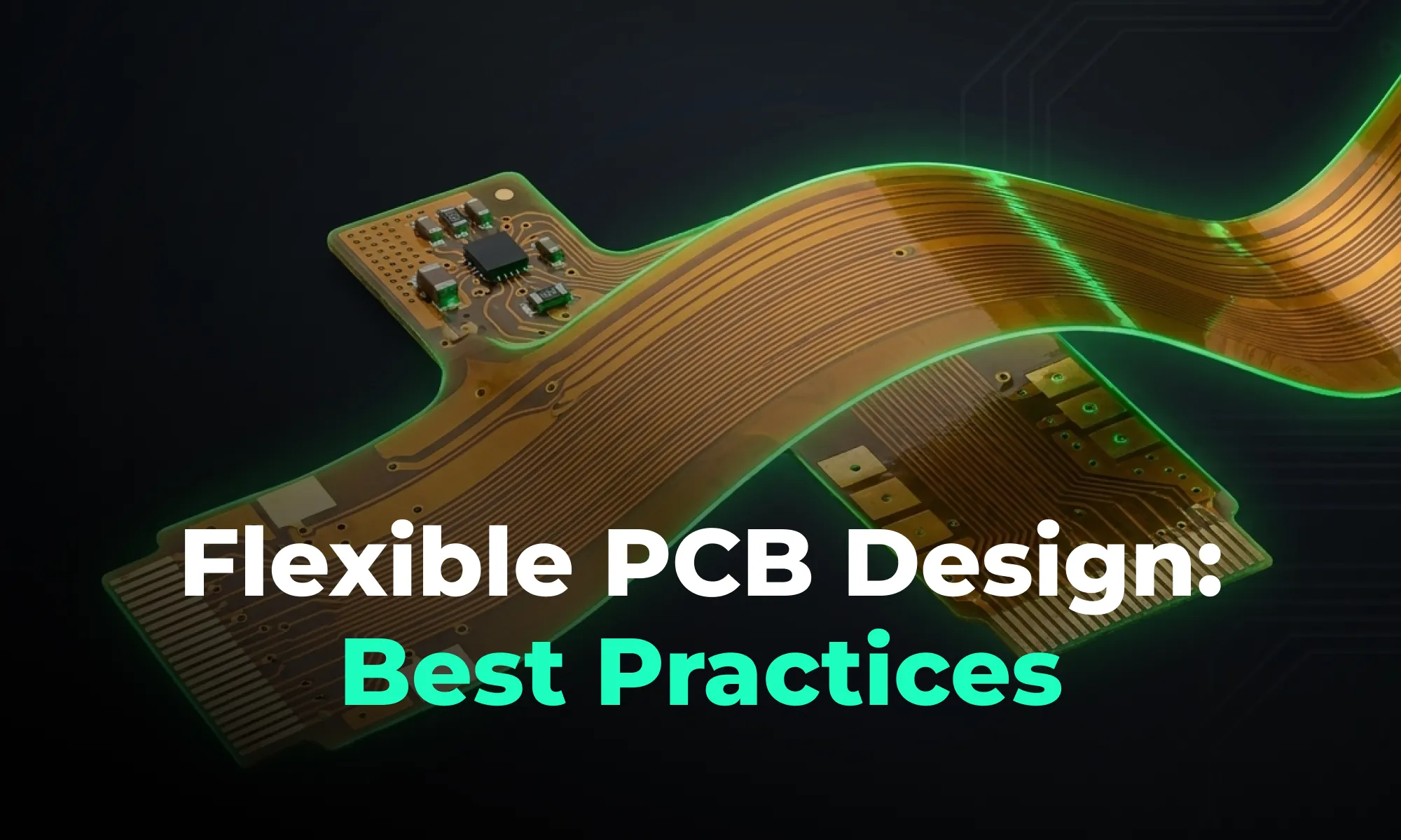
A guide to flexible PCB design, covering materials, stackups, bend radius, and layout best practices for wearables, medical devices, and other compact electronics.

A beginner-friendly guide to reading PCB schematics, covering common symbols, nets, and how to follow signal flow through a circuit diagram.

An overview of collaborative PCB design, showing how cloud-native tools, real-time editing, and shared libraries are reshaping modern hardware team workflows.

A guide to managing PCB component libraries, covering symbols, footprints, and 3D models with best practices for standardizing parts across hardware teams.
