Designing a PCB from scratch can feel like reinventing the wheel. Why start over when you can leverage proven designs, customize them with AI, and let the routing take care of itself?

That's why we're partnering with Seeed Studio. Together, we’re making it incredibly easy to bring your ideas to life.

With Flux, you can start with a ready-made project or a tailored template, customize it using Flux Copilot, and then let AI Auto-Layout handle the rest. Once your design is complete, Seeed takes over, fabricating, assembling, and shipping your project—at no cost.

Start with a Solid Foundation

The Seeed organization in Flux has everything you need to get started:

Ready-to-Clone Projects

These are complete, functional designs you can use as a starting point:

Popular Board Templates

If you’re building something unique, start with one of Seeed’s board templates. These templates include footprints, pinouts, and configurations, so you can get to designing faster without starting from scratch.

Customize with Flux CoPilot

Once you’ve cloned a project or chosen a template, Flux Copilot helps you make it uniquely yours. Adding components, swapping LEDs, or refining connections. You can drop in new parts, and Copilot will automatically guide you through their placement and configuration, ensuring your changes fit seamlessly into the existing design.

  1. Add Components: Drop in new parts and Copilot will help connect and configure them.
  2. Modify the Design: Swap LEDs, add connectors, or tweak pin assignments without the guesswork.
  3. Validate Changes: Copilot provides real-time guidance, ensuring your design stays functional as you customize.

It’s like having an expert engineer on your team, guiding you through each step. Learn more about Copilot.

Let Auto-Layout Do the Heavy Lifting

Once your schematic is complete, it’s time to move on to the layout. Traditionally, this step can be tedious and time-consuming, but Flux’s AI Auto-Layout changes the game. Instead of routing traces manually, Auto-Layout optimizes your board in minutes.

  1. Generate Clean Routing: Auto-Layout finds the optimal paths for your traces based on your design constraints.
  2. Ready for Manufacturing: The result is a clean, manufacturable PCB—done in minutes.

The AI intelligently routes components, generating clean, manufacturable designs with no extra configuration needed. During the optimization process, you’ll see multiple iterations of your design as the AI progressively improves the layout. Once it’s complete, you can review and select your preferred version, with the assurance that every option is optimized for manufacturing.

Bring It to Life with Seeed

Here’s the best part: through the LED Remix Campaign, Seeed will manufacture and assemble your project—for free.

Create an LED-based design using a Seeed XIAO board in Flux, then submit to Seeed. Their Fusion service ensures your board is produced with high-quality standards and ready to use. Flux and Seeed work seamlessly together, with templates and ready-made projects optimized for manufacturing from the start. Export your Gerber files in just one click, and let Seeed handle the rest.

What you get:

  • 2 PCBA Boards: Fabrication, parts, assembly, and shipping included.
  • Free Flux Access: 2 months of full access to Flux.

Start Faster, Iterate Smarter

Ready to design? Here’s how:

  1. Clone a Seeed Project or Template in Flux.
  2. Customize Your Design with Copilot.
  3. Auto-Layout to optimize your PCB in minutes.
  4. Submit to Seeed and get your boards fabricated for free.

With Flux and Seeed, it’s never been easier to design, iterate, and manufacture PCBs. Start faster, and bring your ideas to life.

Profile avatar of the blog author

Nico Tzovanis

Nico is a professional electronics and PCB design engineer at Flux. Find him on Flux @nico

Go 10x faster from idea to PCB
Work with Flux like an engineering intern—automating the grunt work, learning your standards, explaining its decisions, and checking in for feedback at key moments.
Illustration of sub-layout. Several groups of parts and traces hover above a layout.
Design PCBs with AI
Introducing a new way to work: Give Flux a job and it plans, explains, and executes workflows inside a full browser-based eCAD you can edit anytime.
Screenshot of the Flux app showing a PCB in 3D mode with collaborative cursors, a comment thread pinned on the canvas, and live pricing and availability for a part on the board.

Related Content

Component Selection in PCB Design: How Engineers Choose the Right Parts

Component Selection in PCB Design: How Engineers Choose the Right Parts

A guide to PCB component selection, covering electrical specs, footprints, thermal performance, sourcing, and best practices for picking parts that ship reliably.

Profile avatar of Yaneev Hacohen
Yaneev Hacohen
|June 15, 2026
PCB Design Reviews: Best Practices for Catching Errors Early

PCB Design Reviews: Best Practices for Catching Errors Early

A guide to PCB design reviews, covering schematic, layout, and DFM checks engineers use to catch errors early and ship more reliable boards.

Profile avatar of Yaneev Hacohen
Yaneev Hacohen
|June 15, 2026
How to Create and Manage PCB Footprint Libraries

How to Create and Manage PCB Footprint Libraries

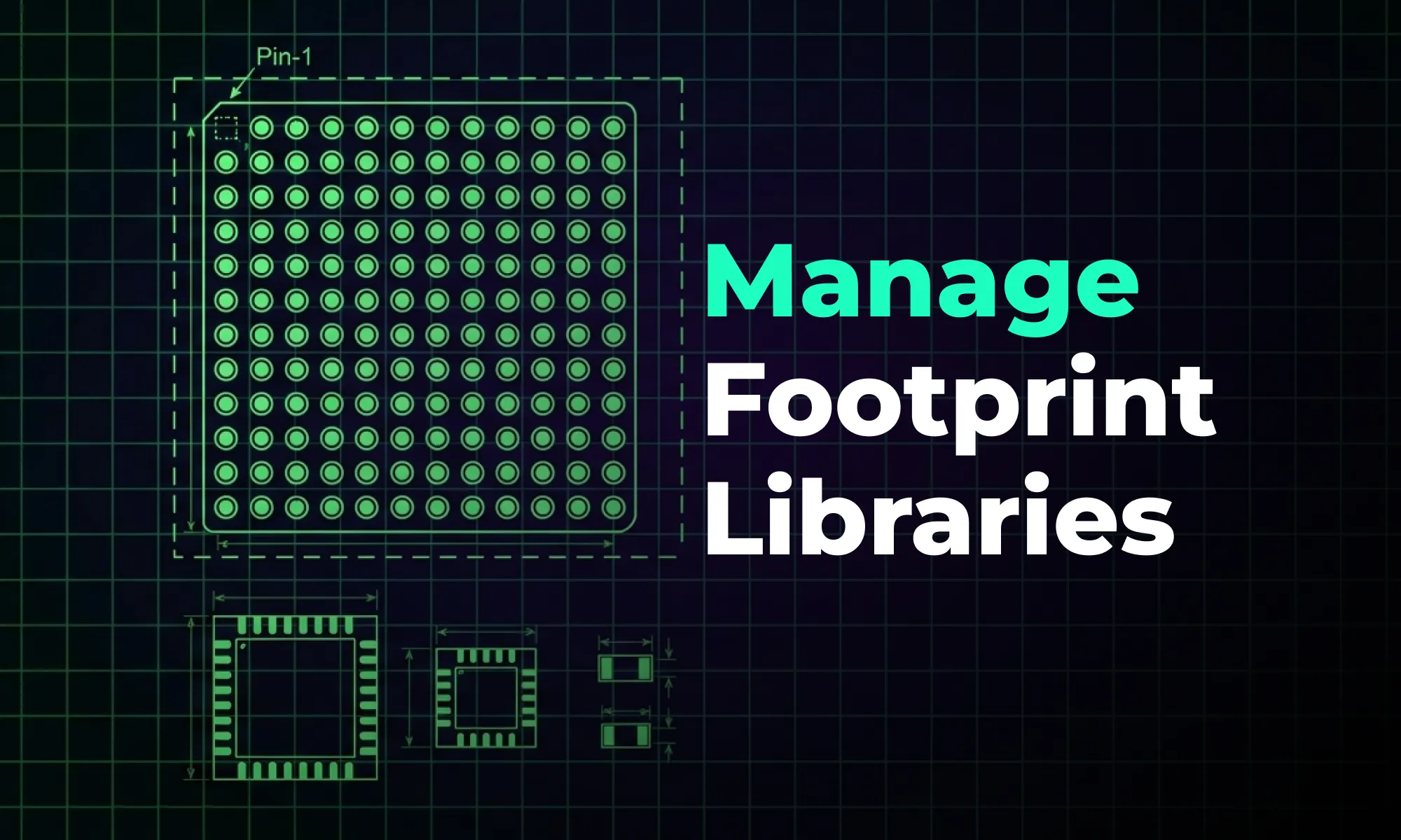
A guide to creating and managing PCB footprint libraries, covering IPC standards, pad sizing, validation workflows, and best practices for reliable land patterns.

Profile avatar of Yaneev Hacohen
Yaneev Hacohen
|June 15, 2026
PCB Schematic Best Practices for Clean Circuit Design

PCB Schematic Best Practices for Clean Circuit Design

A guide to PCB schematic best practices, covering organization, symbols, labeling, and readability tips for clean, maintainable circuit diagrams.

Profile avatar of Yaneev Hacohen
Yaneev Hacohen
|June 15, 2026
Flexible PCB Design Guide: Materials, Layout, and Applications

Flexible PCB Design Guide: Materials, Layout, and Applications

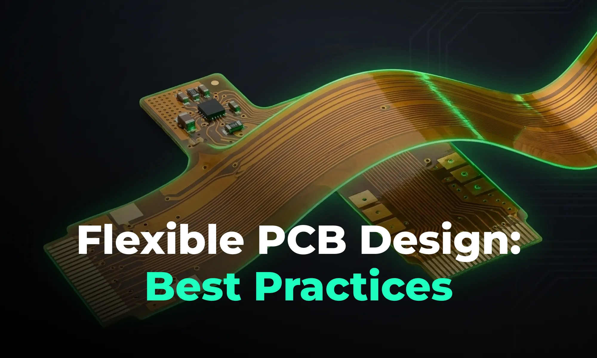
A guide to flexible PCB design, covering materials, stackups, bend radius, and layout best practices for wearables, medical devices, and other compact electronics.

Profile avatar of Yaneev Hacohen
Yaneev Hacohen
|June 8, 2026
How to Read PCB Schematics: A Beginner-Friendly Guide

How to Read PCB Schematics: A Beginner-Friendly Guide

A beginner-friendly guide to reading PCB schematics, covering common symbols, nets, and how to follow signal flow through a circuit diagram.

Profile avatar of Yaneev Hacohen
Yaneev Hacohen
|June 8, 2026
Collaborative PCB Design: Why Hardware Teams Are Moving to the Cloud

Collaborative PCB Design: Why Hardware Teams Are Moving to the Cloud

An overview of collaborative PCB design, showing how cloud-native tools, real-time editing, and shared libraries are reshaping modern hardware team workflows.

Profile avatar of Yaneev Hacohen
Yaneev Hacohen
|June 5, 2026
PCB Component Libraries: Best Practices for Managing Parts

PCB Component Libraries: Best Practices for Managing Parts

A guide to managing PCB component libraries, covering symbols, footprints, and 3D models with best practices for standardizing parts across hardware teams.

Profile avatar of Yaneev Hacohen
Yaneev Hacohen
|June 5, 2026