May 15, 2026
Thermal Management in PCB Design: Methods and Best Practices
Share
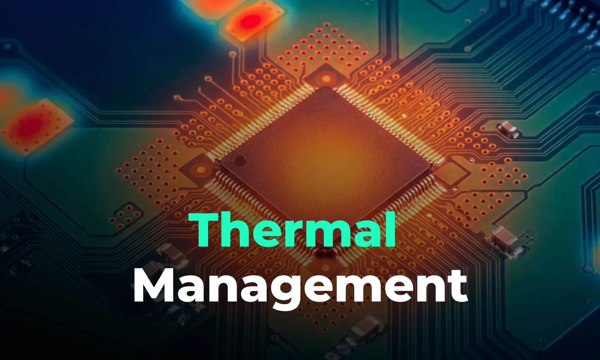
Elevated temperature is the most consistent cause of premature hardware failure: heat accelerates the chemical and mechanical degradation processes inside components in the PCB.
The "10°C increase = half life" rule comes from applying the Arrhenius equation, which relates the rate of chemical reactions to temperature, to failure mechanisms in electronics. It is worth treating this as a rough directional guide rather than a precise law. The rule has been criticized for ignoring significant failure modes unrelated to maximum operating temperature, and the Arrhenius model is only appropriate for certain mechanisms like corrosion and electromigration, not for others such as contact interface stress relaxation or fatigue of package-to-board interconnects.
That said, the practical implication is unchanged: run your board hot and it will fail faster. The failure mechanisms you need to design against include:
Before you can cool a board, you need to locate its thermal sources. Most heat in a printed circuit board (PCB) originates from three predictable places:
Identifying these sources early in the design cycle lets you apply the right mitigation before you've painted yourself into a corner with routing.
Heat moves through three mechanisms: conduction, convection, and radiation. In PCB design, conduction (moving heat through copper) and convection (transferring heat to air) dominate. Engineers typically combine multiple techniques, since no single method covers every scenario.
| Cooling Method | Primary Mechanism | Implementation | Best Used For |
|---|---|---|---|
| Thermal Vias | Conduction | Plated through-holes linking surface pads to internal planes | High-power surface-mount ICs and MOSFETs with exposed thermal pads |
| Copper Pours | Conduction | Wide copper areas acting as heat spreaders | Distributing localized heat across a larger surface area |
| Heat Sinks | Convection | Metal fins attached directly to component packages | Processors and high-power regulators requiring large thermal relief |
| Active Airflow | Convection | Chassis fans pushing air across the board | Enclosed systems where passive convection alone is insufficient |
One thing engineers often miss: a large heat sink is useless if the thermal interface material (TIM) between the chip and the sink has high resistance. The full thermal path from silicon junction to ambient air must be low-resistance at every link in the chain.
Thermal vias are strategically placed plated holes that allow heat to move vertically through the PCB stackup, creating a conductive pathway that spreads thermal energy into internal copper planes or the opposite side of the board. They are most effective under surface-mount devices that feature an exposed thermal pad on their underside, such as quad flat no-lead (QFN) and quad flat package (QFP) parts.
While routing these plated holes directly beneath a hot component is excellent for a thermal management PCB layout, it introduces a physical manufacturing hazard. When you drill open holes into a flat metal surface meant for soldering, those cavities act like tiny straws. During the reflow phase of assembly, capillary action physically pulls the molten solder away from the component pad and down into the via barrel. We call this phenomenon solder wicking.
Because the liquid solder escapes down into the board's internal layers, you are left with insufficient solder coverage on the surface. This creates a weak mechanical attachment and, ironically, a highly resistive thermal connection. You've essentially starved the joint. To solve the solder wicking challenge, hardware teams generally employ two mitigation approaches:
Beyond solder wicking, keep these design rules in mind:
If you leave thermal decisions until the end of the routing phase, you will likely have no room for proper copper pours or heat sinks. Thermal design needs to be a first-class constraint from the moment you start placing components.
Follow this checklist when building thermal reliability into your layout:
When routing high-current paths, keep traces short and thick. Longer traces accumulate more resistance and generate more total heat. For extreme current requirements, specify 2 oz or 3 oz copper on outer layers.
Even experienced engineers make these errors when form factor pressure or signal integrity requirements compete for attention.
Watch for these additional layout errors:
Historically, thermal analysis meant exporting a finished layout to a separate field solver. If the thermal engineer found a hotspot, the hardware engineer had to rip up routing, move components, and restart. This back-and-forth discourages the iterative optimization that good thermal design actually requires.
Modern PCB tools bring constraint management directly into the layout environment. Flux lets teams manage high-speed PCB design rules alongside power constraints from the beginning of the design cycle. By visualizing part placement and tracking net properties in a unified workspace, designers catch thermal bottlenecks before they become routing problems.
Because Flux is cloud-based, a thermal expert can review component placement for airflow optimization while the hardware engineer continues routing signals. That parallel workflow eliminates the redesign loops that plague traditional hardware development.
Ready to put these principles into practice? Try Flux — the browser-based PCB design platform with built-in AI, real-time collaboration, and intelligent design rule checks that help you get your board right the first time.


How hardware teams apply Git-style version control to PCB design — tracking revisions, collaborating safely, and maintaining a complete design history.

A guide to flexible PCB design, covering materials, stackups, bend radius, and layout best practices for wearables, medical devices, and other compact electronics.

A beginner-friendly guide to reading PCB schematics, covering common symbols, nets, and how to follow signal flow through a circuit diagram.
Learn the key differences between analog and digital PCB design and how to manage mixed-signal layouts for better signal integrity.

Learn how to place and select decoupling capacitors to improve power integrity in PCB design.

Learn the core rules of differential pair routing including parallel routing, consistent spacing, length matching, and return path management for high-speed PCB designs.
Learn the most common causes of PCB EMI issues and proven layout, grounding, shielding, and filtering techniques to pass EMC compliance.

Learn the most common PCB testing methods including flying probe and in-circuit testing to ensure reliability.
