April 2, 2026
Flux April 2026 release: upgrades that make a real difference

If you’ve been using Flux week to week, you’ve probably noticed a steady drumbeat of small changes. This release is a snapshot of what we shipped across January to March, the concrete stuff that makes designing in Flux faster, more reliable, and a little less fiddly.
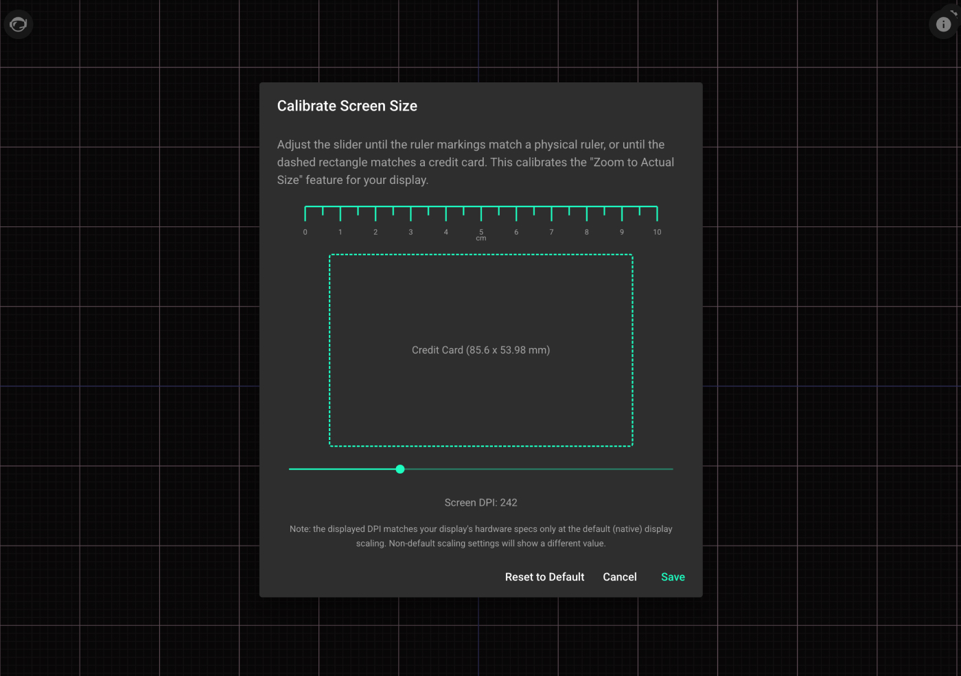
You can now calibrate your screen so components and projects appear at real-world physical scale.
Why it matters: when you’re working in tight mechanical constraints (enclosures, board outlines, connector placement), “close enough” on-screen scale is still friction. Getting to true 1:1 helps you make better placement decisions faster.
We made the editor more responsive and improved undo/redo performance.
Why it matters: when you’re iterating quickly, latency breaks flow. This is the kind of improvement you feel constantly, even if it’s hard to point to one “feature.”
We added a dedicated Layout Rules panel in the Inspector.
Why it matters: rules and constraints are easier to discover and adjust when they’re surfaced where you’re already working. This shortens the loop between “what’s going wrong?” and “fix it.”
Why it matters: It enables a faster and more natural workflow, simply place vias, pads, and silkscreen features right from the context menu accessible by right clicking on the PCB canvas.
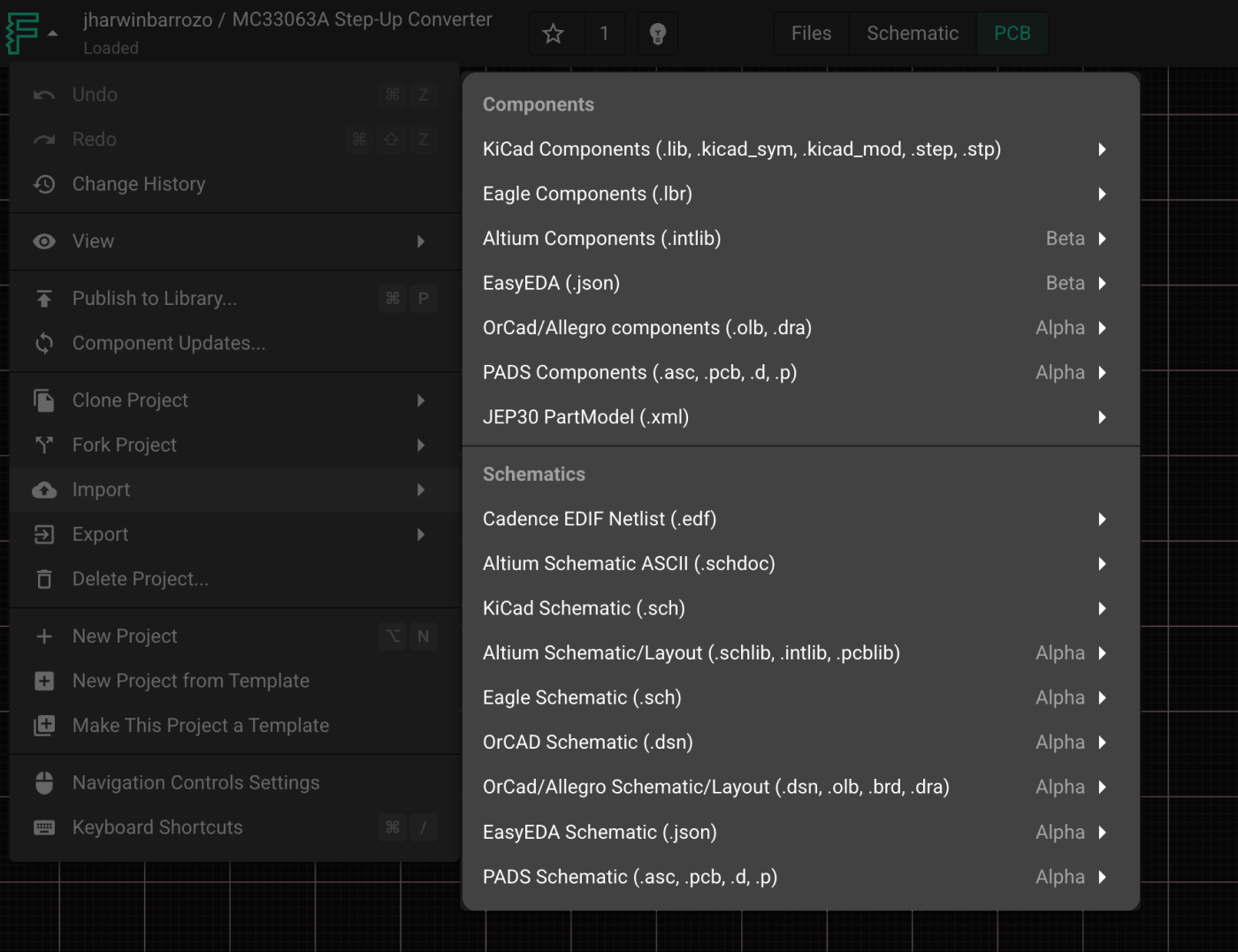
You can import Eagle schematic files (.sch) into Flux and keep them editable.
Why it matters: migration is only useful if you can keep working once you land. This makes Flux a more practical option for teams with real legacy designs.
Flux now supports importing PADS ASCII footprints.
Why it matters: footprints are often the blocker when moving between tools. Every new import path reduces busywork and makes it easier to reuse what you already trust.
We improved Flux Chat’s ability to stay stable and usable in longer threads.
Why it matters: when an assistant loses context (or becomes slow) mid-task, it’s not just annoying — it breaks the workflow. The goal here is: you should be able to keep going without “resetting” the conversation.
We made simulator chats stay responsive as threads get longer.
Why it matters: simulation is iterative. You shouldn’t have to restart the loop just because you’ve been working for a while.
AI Agent now does more cleanup work automatically before it finishes.
Why it matters: the best automation removes the boring steps without you having to babysit it. This is one of those changes that turns “AI could help here” into “AI did help here.”
Flux now supports the placement of pins on top and bottom of parametric pins by specifying the Pin Orientation property.
Why it matters: This allows users to create clean and readable symbols.
Why it matters: Pad numbers don’t have to manually entered for each Terminal anymore speeding up the workflow greatly.
Why it matters: Certain properties are required for a high-quality BOM. We now automatically add Manufacturer Part Number, Manufacturer Name, Part Type, Datasheet URL, and Designator Prefix to ensure a strong baseline across symbols.
Flux is moving fast. The goal isn’t change for change’s sake — it’s to keep tightening the loop: faster iteration, fewer workflow breaks, and better support for the formats and tools you already use.
If there’s a part of your day-to-day flow that still feels slower than it should (or a paper cut you hit every session), tell us. Those are often the highest-leverage fixes, and they’re exactly what we’re prioritizing.


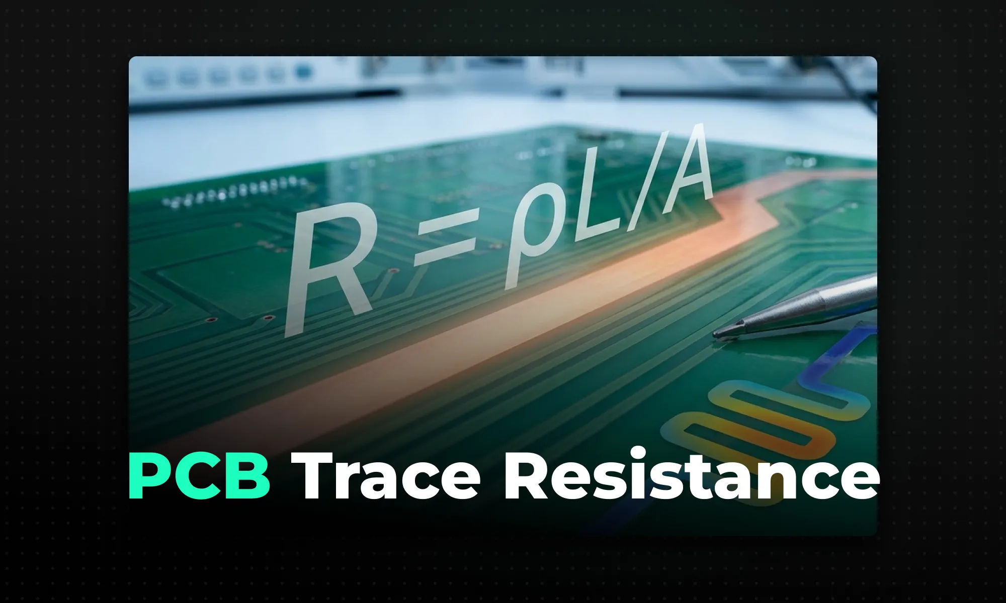
A practical guide to calculating PCB trace resistance, covering the core formula, how geometry affects resistance, worked examples, and design tips to minimize voltage drop and heat.

A practical guide to diagnosing and fixing PCB failures, covering common symptoms, a step-by-step debugging workflow, essential tools (multimeter, oscilloscope, logic analyzer, thermal camera), a pre-power-up checklist, and the design mistakes that most often lead to broken boards.
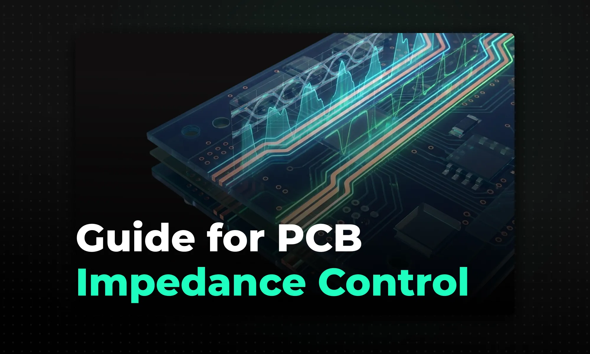
A practical guide to PCB impedance control, covering why it matters for signal integrity, the four physical variables that shape trace impedance, and how to enforce impedance targets from stackup planning through routing and fabrication.
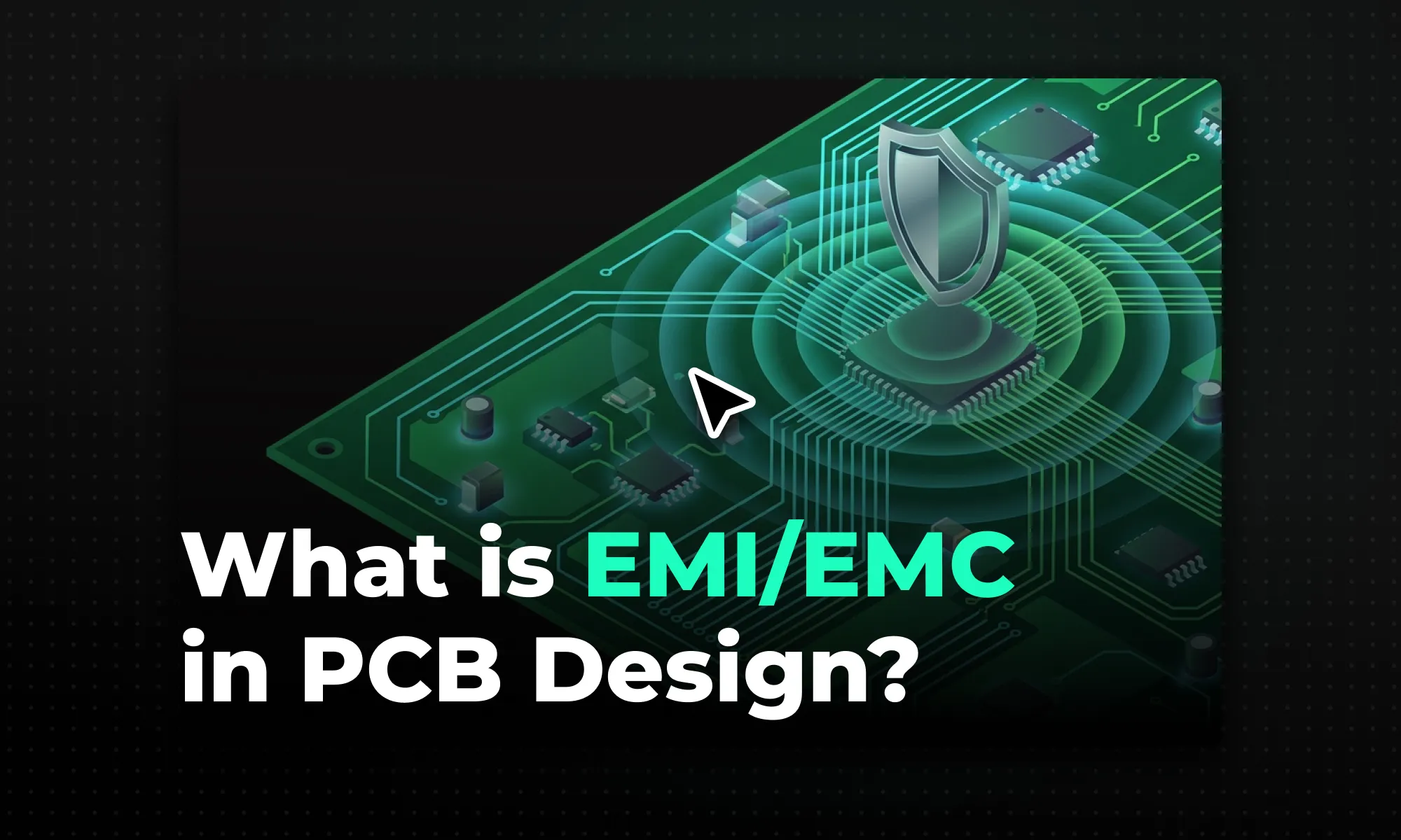
A practical guide to reducing EMI in PCB design through grounding, return path control, shielding, and layout best practices. Covers EMC compliance with CISPR 32 and FCC Part 15.
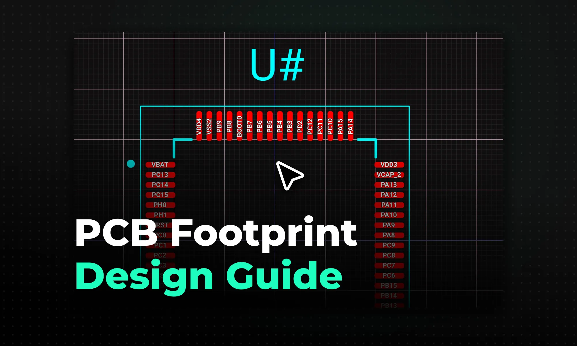
A step-by-step guide to designing accurate PCB footprints — covering pads, silkscreen, courtyards, IPC-7351 density levels, origin setup, and common mistakes to avoid.

A practical guide to PCB grounding techniques — ground planes, return paths, star grounding, and analog/digital partitioning — with best practices for reducing noise and improving signal stability.
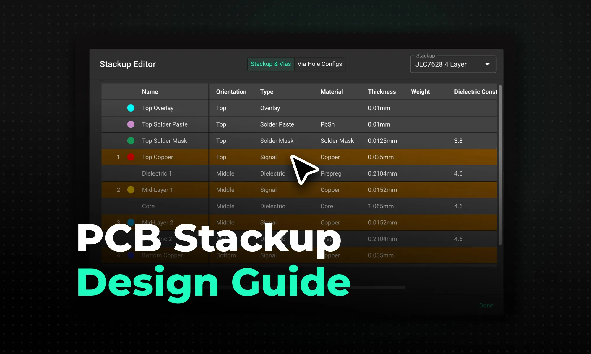
A practical guide to designing multilayer PCB stackups for signal integrity, EMI control, and stable power delivery. Covers layer types, controlled impedance, common mistakes, and how modern tools simplify the process.
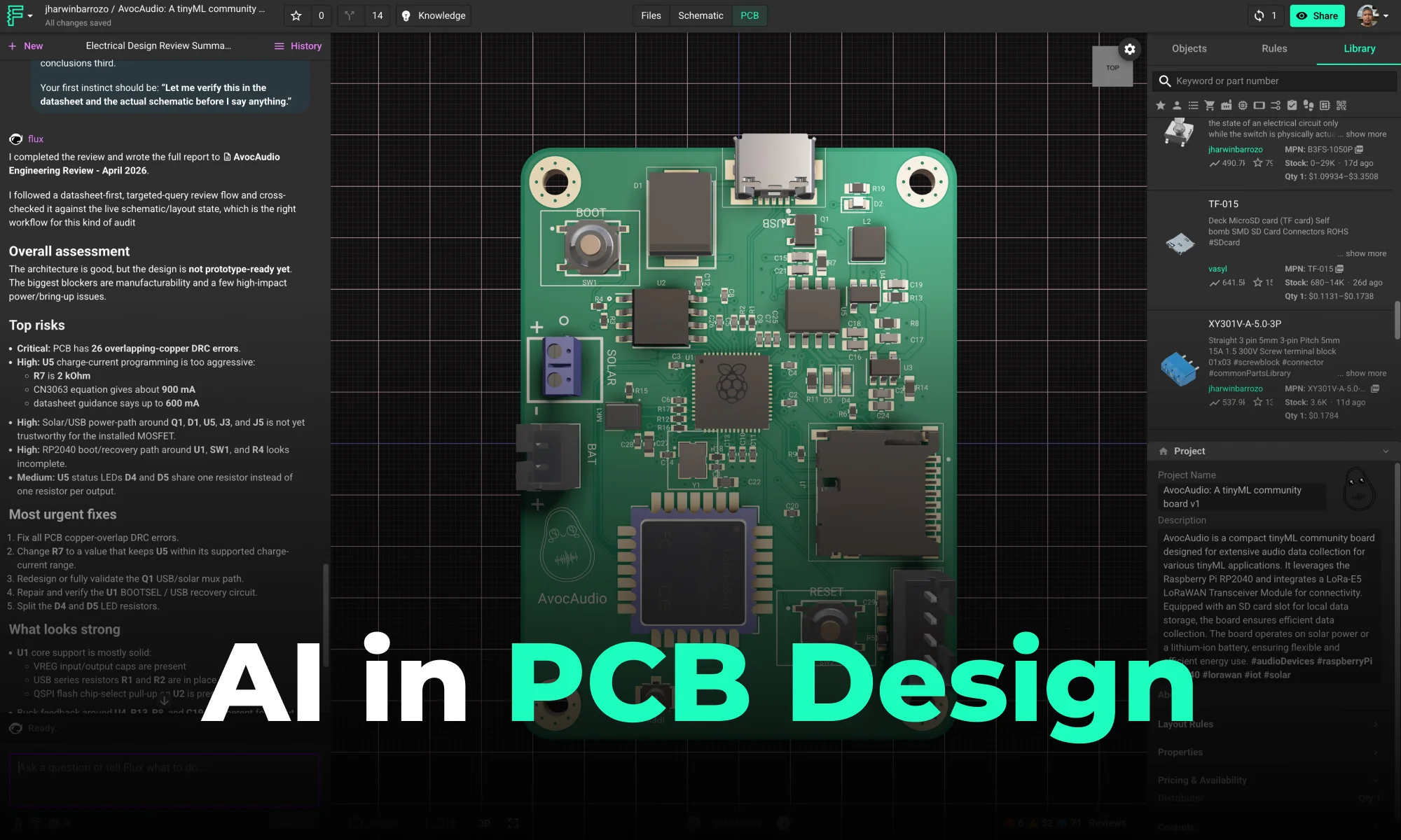
A look at how AI is reshaping PCB design by automating routing, placement, and signal integrity checks so engineers can focus on architecture and higher-level decisions.