May 6, 2026
Electronic Circuit Design Explained: From Schematics to PCB Layout
Share

Electronic circuit design is the process of creating a blueprint that dictates how electrical signals power a device. Every hardware project starts here, before a single component is purchased or a board is fabricated. If you get the design wrong at this stage, you'll pay for it in numerous board re-spins.
There are three primary circuit categories you'll encounter:
| Signal Type | Definition | Common Thresholds (Logic 0 / Logic 1) |
|---|---|---|
| Analog | Continuous variable voltage or current | N/A (continuous spectrum) |
| Digital (TTL) | Discrete binary signal using Transistor-Transistor Logic | 0V to 0.8V / 2.0V to 5.0V |
| Digital (CMOS, 5V) | Discrete binary signal using Complementary Metal-Oxide Semiconductor | 0V to 1.5V / 3.5V to 5.0V |
Note: CMOS thresholds scale with supply voltage (typically 30–70% of Vcc). Always verify against the component datasheet.
Every schematic is built from a small set of fundamental building blocks. Know what each one does before you start placing symbols.
A schematic circuit diagram is a logical representation of electrical connections, not a physical map of the board. Engineers use schematics to define component relationships using standardized symbols, with drawn lines called nets representing the intended flow of signals across the system.
A schematic only holds value if it accurately represents the intended electrical behavior without logical errors. Achieving a verified schematic means thoroughly checking all net connections and assigning accurate component models. Before moving to physical layout, a verified schematic lets you run simulation to validate analog behavior and signal integrity. Simulation Program with Integrated Circuit Emphasis (SPICE) is the industry standard for analog electronic circuit simulation — you provide a netlist of the circuit you wish to simulate, and SPICE generates waveform plots for analysis.
For high-speed digital interfaces specifically, designs concerned with signal integrity, drive strength, or transmission line errors at digital I/O pins benefit from Input/Output Buffer Information Specification (IBIS) models. Both tools are complementary, not competing: SPICE dominates analog verification, while IBIS handles high-speed digital signal behavior at the board level.
Once your logical blueprint is verified, you translate it into a physical board. PCB layout design determines where each component sits and how copper traces connect them, and the decisions you make here directly affect signal integrity, thermal performance, and manufacturability.
The transition from logical to physical requires managing real electrical constraints. You group logical blocks during placement, route copper traces to complete your nets, configure the board stackup for your signal speeds, and run Design Rule Checks (DRC) to catch clearance violations before you send files to the fabricator.
Forward and back annotation between the schematic and PCB layout ensures continuous synchronization of reference designators, footprints, and connectivity, minimizing the risk of mismatches during design iteration. Skipping this synchronization step is one of the most common causes of costly late-stage re-spins.
Hardware design is not a single linear step. It's a lifecycle that moves a concept from a requirements document to a manufacturable physical object, with multiple revision cycles along the way.
The number of prototype iterations depends on design complexity. Simple digital designs may move to production after one validated build, while high-speed, RF, HDI, or mixed-signal platforms may require multiple iterations to fine-tune impedance, thermal performance, or routing density.
Early boards expose signal integrity challenges, placement constraints, thermal behavior, and design-for-manufacturing (DFM) considerations before they become costly production issues.
Theoretical designs fail in the real world for predictable reasons. The gap between a clean schematic and a working board comes down to parasitic effects, unmitigated high-frequency phenomena.
Electromagnetic interference (EMI) and signal noise corrupt data lines when high-speed traces lack proper return paths. Power delivery network (PDN) instability is another common failure mode, misplaced decoupling capacitors cause integrated circuits to drop voltage and reset unexpectedly under load. Improper grounding is one of the most frequent causes of noise, signal distortion, and EMI issues, with common mistakes including floating grounds, ground loops, and inadequate ground plane segmentation.
Traditional electronic design automation (EDA) software relies on disconnected desktop applications. That methodology creates file versioning conflicts, slows design reviews, and isolates the schematic engineer from the layout designer. The handoff between tools becomes a bottleneck, and every bottleneck is a place where errors hide.
Modern platforms like Flux move the entire PCB schematic design workflow to a cloud-based environment. The result is fewer friction points between design stages and faster iteration cycles.
Hardware teams adopting AI tools are reporting fewer board spins, with early schematic linting catching mismatched nets and mis-assigned pins before layout — one aerospace supplier reported a 30 percent reduction in re-spins within the first year.
Ready to move your hardware projects out of the concept phase and onto the test bench? Proper electronic circuit design is much faster when your tools actively assist you rather than getting in your way. Take the next step by trying Flux, where real-time collaboration, a massive community part library, and a smart AI Copilot bring your schematics and PCB layouts to life all in one browser tab.


A guide to PCB component selection, covering electrical specs, footprints, thermal performance, sourcing, and best practices for picking parts that ship reliably.
A guide to PCB design reviews, covering schematic, layout, and DFM checks engineers use to catch errors early and ship more reliable boards.
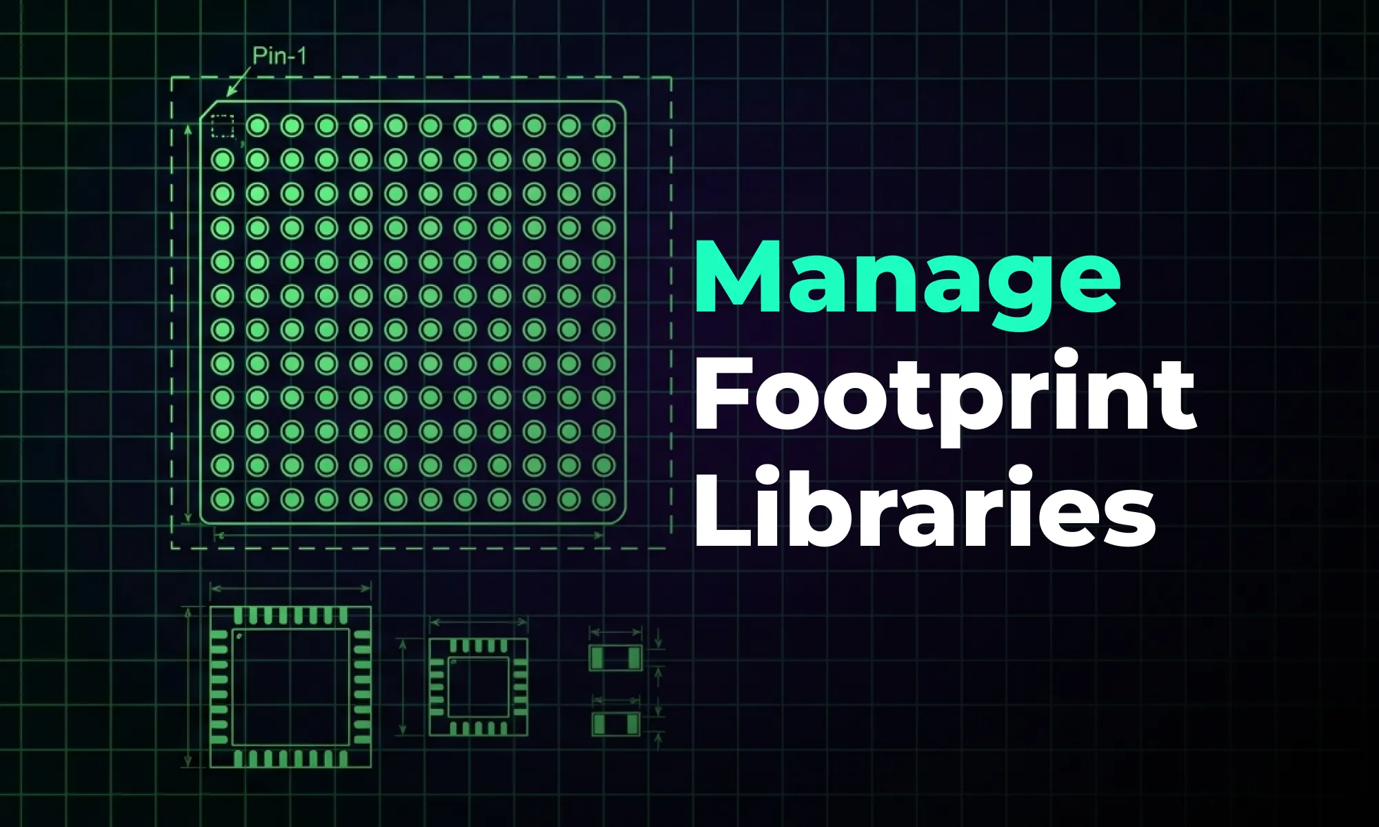
A guide to creating and managing PCB footprint libraries, covering IPC standards, pad sizing, validation workflows, and best practices for reliable land patterns.

A guide to PCB schematic best practices, covering organization, symbols, labeling, and readability tips for clean, maintainable circuit diagrams.

A guide to flexible PCB design, covering materials, stackups, bend radius, and layout best practices for wearables, medical devices, and other compact electronics.

A beginner-friendly guide to reading PCB schematics, covering common symbols, nets, and how to follow signal flow through a circuit diagram.

An overview of collaborative PCB design, showing how cloud-native tools, real-time editing, and shared libraries are reshaping modern hardware team workflows.

A guide to managing PCB component libraries, covering symbols, footprints, and 3D models with best practices for standardizing parts across hardware teams.
