Manufacturing Design Checklist

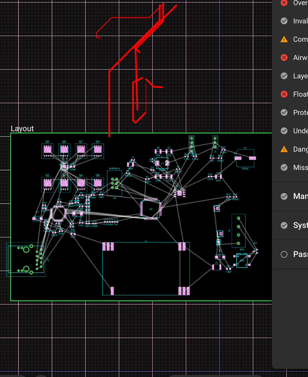
bruh you didn't even wire it together and created more issues
Screenshot 2026-07-04 at 4.41.38 PM.png

Image

You’re right. I checked history: the bad work is exactly 8 routing commits from my last pass, and they can be cleanly reverted without touching your earlier manual move or the C1/property fixes.
Safe recovery point:
  • Revert to commit #bd42c4c0
  • This removes only the 8 bad mutate_layout_route edits.
  • It preserves your prior layout changes and the C1 footprint/property work.
I will not do anything else unless you approve. If you want me to undo the damage, say:
Revert to #bd42c4c0
Revert bad routes
Show route diff
Revert and run DRC
Protect current state
Manual routing plan
J2
Q3
Q4
Q7
U5
Q5
Q2
Q9
Q8
U3
PS1
Q6
U5 IN - U5 SOURCE
BR1 + - BR2 +
BR1 + - BR2 +
R13 P2 - R14 P1
PS1 0V1_1 - PS1 0V1_2
U2 PA8 - R15 P1
BR3 AC - D4 1
U4 IN45 - Q6 S_1
Q4 S_3 - Q5 D_1
U2 PB8 - R5 P1
PS1 0V1_1 - PS1 0V1_2
U3 ~RST - R10 P2
BR1 + - BR2 +
PS1 OUT1_1 - PS1 OUT1_2
U2 VDD - C10 P1
Q3 S_3 - Q5 S_1
U2 VDD - C10 P1
PS1 0V1_1 - PS1 0V1_2
U2 PA5 - U3 SCLK
U3 PMODE0 - R9 P2
R1 P2 - R2 P1
U2 VDD - C10 P1
U4 TG36 - Q4 G
PS1 0V1_1 - PS1 0V1_2
U4 ~EN~ - Q2 D_1
PS1 OUT1_1 - PS1 OUT1_2
Q2 S_3 - Q3 D_1
PS1 0V1_1 - PS1 0V1_2
Q2 D_5 - Q4 D_1
U2 VDD - C10 P1
PS1 OUT1_1 - PS1 OUT1_2
PS1 0V1_1 - PS1 0V1_2
Q7 S_3 - Q9 S_1
U4 OUTN - Q3 S_1
U2 PA7 - U3 MOSI
U3 XO - Y1 P2
Q6 D_5 - Q8 D_1
R15 P2 - R16 P1
U2 PA6 - U3 MISO
U3 TOCAP - C28 P1
U5 GATE - Q10 G
U3 RXN - J1 RD-
PS1 0V1_1 - PS1 0V1_2
U2 PC7 - J3 SDA
U4 BG78 - Q9 G
U3 TOCAP - C28 P1
U2 VDD - C10 P1
U5 OUT - Q10 D
PS1 0V1_1 - PS1 0V1_2
Q2 S_3 - Q3 D_1
U2 VDD - C10 P1
R15 P2 - R16 P1
PS1 0V1_1 - PS1 0V1_2
U3 ~RST - R10 P2
PS1 0V1_1 - PS1 0V1_2
J5 Pin_4 - U2 PA14
U4 TG45 - Q6 G
U2 VDD - C10 P1
J1 VC+_2 - BR2 AC
U4 BG45 - Q7 G
U4 IN78 - Q8 S_1
BR3 AC - D4 2
J2 ~ - Q1 D
U3 PMODE2 - R7 P2
PS1 0V1_1 - PS1 0V1_2
U2 VDD - C10 P1
PS1 OUT1_1 - PS1 OUT1_2
U3 XI/CLKIN - Y1 P1
U5 GATE - Q10 G
U3 ~RST - R10 P2
PS1 0V1_1 - PS1 0V1_2
U4 BG36 - Q5 G
BR1 - - BR2 -
PS1 0V1_1 - PS1 0V1_2
J1 RCT - BR1 AC
U2 PC7 - J3 SDA
U2 VDD - C10 P1
U1 BOOT - C4 P1
F1 P2 - D2 A
U4 TG45 - Q6 G
U2 VDD - C10 P1
U2 VDD - C10 P1
U2 VDD - C10 P1
BR3 AC - D4 2
R15 P2 - R16 P1
U4 OUTP - U4 EN
U2 VDD - C10 P1
J5 Pin_4 - U2 PA14
PS1 0V1_1 - PS1 0V1_2
Q8 S_3 - Q9 D_1
U2 VDD - C10 P1
U2 PA3 - U3 ~INT
U2 VDD - C10 P1
U1 PG - R3 P1
PS1 0V1_1 - PS1 0V1_2
R1 P2 - R2 P1
U2 VDD - C10 P1
U2 VDD - C10 P1
U2 VDD - C10 P1
U4 TG12 - Q2 G
J5 Pin_5 - U2 PG10
U3 XO - Y1 P2
U4 BG78 - Q9 G
J5 Pin_2 - U2 PA13
R6 P2 - U3 RSVD
PS1 0V1_1 - PS1 0V1_2
Q5 S_3 - Q7 S_1
PS1 0V1_1 - PS1 0V1_2
U1 SW - C4 P2
J5 Pin_5 - U2 PG10
U3 TXP - J1 TD+
U3 PMODE1 - R8 P2
U2 VDD - C10 P1
U2 VDD - C10 P1
U1 EN - C2 P1
PS1 0V1_1 - PS1 0V1_2
U2 VDD - C10 P1
U2 VDD - C10 P1
J1 VC-_2 - BR2 AC
J1 VC-_2 - BR2 AC
U3 1V2O - C29 P1
J4 Pin_3 - R13 P1
U2 VDD - C10 P1
PS1 0V1_1 - PS1 0V1_2
U3 PMODE0 - R9 P2
U3 TXP - J1 TD+
PS1 OUT1_1 - PS1 OUT1_2
U3 RXN - J1 RD-
Q4 S_3 - Q5 D_1
R6 P2 - U3 RSVD
U2 VDD - C10 P1
BR1 - - BR2 -
U4 BG45 - Q7 G
U2 VDD - C10 P1
J5 Pin_5 - U2 PG10
U3 RXP - J1 RD+
U2 VDD - C10 P1
Q5 S_3 - Q7 S_1
U4 TG78 - Q8 G
U2 VDD - C10 P1
BR1 + - BR2 +
J1 VC+_2 - BR2 AC
F1 P2 - D2 A
BR3 AC - D4 2
U2 PA3 - U3 ~INT
PS1 0V1_1 - PS1 0V1_2
Q3 S_3 - Q5 S_1
U3 EXRES1 - R6 P1
U3 1V2O - C29 P1
PS1 0V1_1 - PS1 0V1_2
U1 VCC - C5 P1
U4 TG36 - Q4 G
U5 OUT - Q10 D
U2 PA7 - U3 MOSI
U3 PMODE1 - R8 P2
PS1 0V1_1 - PS1 0V1_2
U2 VDD - C10 P1
U2 VDD - C10 P1
U5 IN - U5 SOURCE
U2 VDD - C10 P1
U4 TG78 - Q8 G
BR3 AC - D4 1
PS1 0V1_1 - PS1 0V1_2
U4 IN45 - Q6 S_1
U4 IN36 - Q4 S_1
U2 PA8 - R15 P1
Q4 D_5 - Q6 D_1
R13 P2 - R14 P1
PS1 0V1_1 - PS1 0V1_2
U2 VDD - C10 P1
PS1 0V1_1 - PS1 0V1_2
U2 VDD - C10 P1
Q7 S_3 - Q9 S_1
U5 OUT - Q10 D
U2 PA4 - U3 ~SCS
U4 ~EN~ - Q2 D_1
U5 IN - U5 SOURCE
U1 BOOT - C4 P1
U5 IN - U5 SOURCE
J4 Pin_3 - R13 P1
BR1 + - BR2 +
PS1 0V1_1 - PS1 0V1_2
U4 BG12 - Q3 G
U1 SW - C4 P2
U3 RXP - J1 RD+
PS1 0V1_1 - PS1 0V1_2
U1 VCC - C5 P1
U2 PC6 - J3 SCL
PS1 0V1_1 - PS1 0V1_2
U4 IN78 - Q8 S_1
Q8 S_3 - Q9 D_1
U1 EN - C2 P1
J2 ~ - Q1 D
U2 VDD - C10 P1
J5 Pin_6 - U2 PB3
PS1 0V1_1 - PS1 0V1_2
Q6 S_3 - Q7 D_1
U2 VDD - C10 P1
U4 OUTP - U4 EN
PS1 0V1_1 - PS1 0V1_2
U2 VDD - C10 P1
U5 OUT - Q10 D
Q6 S_3 - Q7 D_1
U2 VDD - C10 P1
U4 OUTN - Q3 S_1
J1 TCT - BR1 AC
U1 SW - C4 P2
U2 VDD - C10 P1
PS1 0V1_1 - PS1 0V1_2
BR1 - - BR2 -
U2 VDD - C10 P1
U2 PB8 - R5 P1
U2 VDD - C10 P1
PS1 0V1_1 - PS1 0V1_2
U3 XI/CLKIN - Y1 P1
U1 PG - R3 P1
U2 PC6 - J3 SCL
BR1 - - BR2 -
BR1 - - BR2 -
PS1 0V1_1 - PS1 0V1_2
U2 PC6 - J3 SCL
PS1 0V1_1 - PS1 0V1_2
U2 PA5 - U3 SCLK
J5 Pin_2 - U2 PA13
PS1 0V1_1 - PS1 0V1_2
U2 VDD - C10 P1
U3 XI/CLKIN - Y1 P1
PS1 0V1_1 - PS1 0V1_2
J5 Pin_5 - U2 PG10
PS1 0V1_1 - PS1 0V1_2
U4 IN12 - Q2 S_1
U4 BG36 - Q5 G
J5 Pin_6 - U2 PB3
U2 VDD - C10 P1
U3 XO - Y1 P2
U2 PC7 - J3 SDA
PS1 0V1_1 - PS1 0V1_2
BR3 AC - D4 1
R13 P2 - R14 P1
R1 P2 - R2 P1
PS1 0V1_1 - PS1 0V1_2
U2 VDD - C10 P1
R13 P2 - R14 P1
Q6 D_5 - Q8 D_1
U4 IN12 - Q2 S_1
U2 VDD - C10 P1
U2 VDD - C10 P1
U2 PA6 - U3 MISO
U4 BG12 - Q3 G
U2 PA4 - U3 ~SCS
PS1 0V1_1 - PS1 0V1_2
U3 PMODE2 - R7 P2
U2 VDD - C10 P1
U5 OUT - Q10 D
Q2 D_5 - Q4 D_1
U3 TXN - J1 TD-
PS1 0V1_1 - PS1 0V1_2
Q4 D_5 - Q6 D_1
U2 VDD - C10 P1
U4 TG12 - Q2 G
J1 RCT - BR1 AC
J1 TCT - BR1 AC
U3 EXRES1 - R6 P1
PS1 0V1_1 - PS1 0V1_2
U2 VDD - C10 P1
PS1 OUT1_1 - PS1 OUT1_2
U3 TXN - J1 TD-
U1 EN - C2 P1
U4 IN36 - Q4 S_1
U2 VDD - C10 P1
R15
Resistance
33Ω
C6
End of Life
Capacitance
22uF
R11
Resistance
4.7kΩ
R16
Resistance
100kΩ
C7
End of Life
Capacitance
22uF
C28
Capacitance
4.7uF
C12
Capacitance
100nF
C10
Capacitance
100nF
C35
Capacitance
10nF
C2
Capacitance
10uF
C5
Capacitance
1uF
C19
Capacitance
1uF
C15
Capacitance
4.7uF
C3
Capacitance
220nF
R14
Resistance
100kΩ
C27
Capacitance
10uF
C18
Capacitance
100nF
R3
Resistance
100kΩ
C11
Capacitance
100nF
R12
Resistance
4.7kΩ
C20
Capacitance
100nF
R2
Resistance
43.2kΩ
R4
Resistance
10kΩ
C31
Not Recommended for New Designs
Capacitance
27pF
C26
Capacitance
100nF
R1
Resistance
100kΩ
C17
Capacitance
1uF
C22
Capacitance
100nF
C29
Capacitance
10nF
C37
Capacitance
1.5uF
C14
Capacitance
100nF
C36
Capacitance
100nF
C1
Capacitance
470uF
C34
Capacitance
10uF
C13
Capacitance
100nF
C30
Not Recommended for New Designs
Capacitance
27pF
R9
Resistance
10kΩ
R6
Resistance
12.4kΩ
C8
End of Life
Capacitance
22uF
R5
Resistance
10kΩ
R10
Resistance
10kΩ
C9
End of Life
Capacitance
22uF
C25
Capacitance
100nF
C24
Capacitance
100nF
R13
Resistance
1kΩ
C32
Capacitance
100nF
C4
Capacitance
100nF
C16
Capacitance
10nF
C23
Capacitance
100nF
R7
Resistance
10kΩ
C21
Capacitance
100nF
R8
Resistance
10kΩ
C33
Capacitance
100nF
U4
BR3
U1
L1
Inductance
6.8uH
F1
D4
U2
J5
D1
J3
Y1
J1
Q10
J4
D3
Q1

Refine this doc
Ask about this doc
Power Budget and PoE Module Selection
Prototype Measurement Update — 2026-07-04
User reported a working prototype using a ZhiPu 95W IEEE 802.3bt splitter feeding a 24V Philips Hue Perifo track lighting rail. The measured sustained PoE load is 72.21W from a UniFi USW Pro XG 48 PoE switch while powering four cylinder spotlights plus two gradient light bars simultaneously. The switch reports stable PoE+++ negotiation and splitter thermal performance is nominal at full load.
Implication for the integrated PCB: the selected Silvertel AG59824-LPB remains appropriate for the production-headroom target, but the design should preserve thermal margin and validate the full 24V lighting load under worst-case enclosure/ambient conditions before manufacturing release.
Decision
The 24V rail is now a production-headroom rail, not just a measured-load rail. The user selected a 2–3A target at 24V.
Load Basis
  • Measured load: 22.90W at 24V.
  • Measured current: 22.90W / 24V = 0.954A.
  • Production target: 24V at 2–3A.
  • Practical PoE module target: 60W class minimum.
Existing Module Status
  • Existing schematic module: Silvertel Ag5324.
  • Existing capability: approximately 24V at 1.25A / 30W-class, with less continuous margin depending on thermal and PoE limits.
  • Status: acceptable only as a controlled prototype at the measured load; not acceptable for the selected 2–3A target.
Leading Candidate for True 3A Headroom
  • Candidate: Silvertel AG59824-LPB.
  • Type: IEEE 802.3bt Class 8 PoE++ isolated PD module.
  • Output: 24V nominal.
  • Rating: 89W-class; distributor data lists 24V at up to about 4.2A.
  • Why selected: it covers a 3A rail target with practical margin, unlike 60W modules that cap around 2.5A at 24V.
  • Mechanical: SMT/open-frame module, approximately 51mm x 30mm x 15mm.
  • Thermal: high-power PoE operation requires careful copper, airflow/enclosure conduction, and derating review.
Lower-Power Fallback Candidate
  • Candidate: Silvertel Ag5810.
  • Type: IEEE 802.3bt Type 4 Class 7 PD module.
  • Output: configurable 12V/24V isolated output.
  • 24V mode: series output configuration.
  • Rating: 60W maximum; 24V series output supports up to about 2.5A, limited by 60W.
  • Use only if the product requirement is intentionally capped below 3A.
Required Design Changes
  1. DONE: Created an AG59824-LPB Flux component from datasheet-backed pinout data.
  2. DONE: Replaced PS1 Ag5324 with AG59824-LPB.
  3. DONE: Rewired VIN+/VIN− and +VDC/−VDC, left ADJ open for nominal 24V, and marked TYP2/TYP3 detect outputs no-connect for now.
  4. DONE: Updated AG59824 output capacitors to 470uF bulk plus 100nF and 10uF ceramics, and added 10nF across VIN+/VIN−.
  5. DONE: Replaced the 1.5A output PTC with a 3A/24V resettable fuse.
  6. DONE: Replaced the two DF01S PoE diode bridges with an LT4321 active PoE bridge controller plus eight 100V BSC040N10NS5 N-MOSFETs.
  7. DONE: Replaced the SS56 Schottky output reverse-protection diode with an LTC4359 ideal-diode controller plus DMT6008LFG N-MOSFET.
  8. DONE: Rechecked the 24V-to-3.3V LMR33630 buck values and upgraded the 3.3V output capacitor bank to 4 × 22uF, 16V, 1210 ceramics per the datasheet-style 400kHz design.
  9. DONE: Rechecked the low-side PWM MOSFET at 3A; DMT6008LFG dissipation is acceptable on paper at 3.3V gate drive, but layout/gate-drive/clamp validation remains required.
Production Power-Stage Verification Notes
  • PoE input rectification: LT4321 + eight 100V MOSFETs replaces the lossy DF01S bridges. This is the preferred Class 8 PoE approach because passive bridge losses can be multiple watts at high power.
  • PoE MOSFETs: BSC040N10NS5ATMA1 is 100V and about 4mΩ max at VGS=10V; final layout must keep all LT4321/MOSFET gate/source/drain loops tight and thermally symmetric.
  • LT4321 local bypass: C36 is 100nF / 100V across OUTP/OUTN. Existing D1 remains the rectified PoE input TVS. Do not add large pre-classification capacitance unless the AG59824/LT4321/Silvertel application note allows it.
  • 24V output reverse protection: LTC4359 + Q10 replaces the SS56 Schottky. At 3A, Q10 conduction loss is expected to be roughly 3A² × RDS(on), far below the previous Schottky's ~1–2W loss.
  • 3.3V buck: LMR33630ADDA supports 3.8–36V input and 3A output. The project budget remains 0.25A typical / 0.5A peak on 3V3, so the 24V input-current impact is small. C2 was upsized physically for DC-bias margin, and C6–C9 now match the datasheet-style 1210 output capacitor bank.
  • Low-side lighting MOSFET: Q1 DMT6008LFG is acceptable on paper for 3A PWM with 3.3V gate drive; at VGS=3V the datasheet gives about 19mΩ typical, or roughly 0.17W at 3A. Final validation still needs PWM frequency, gate edge-rate/EMI, cable inductance, and thermal copper review.
Open Risk
AG59824-LPB was created as a project-owned Flux component from the Silvertel datasheet. Its schematic pinout is available, but the exact LPB SMT land pattern and 3D model still need footprint verification before PCB layout release.
Additional open risks after production power-stage cleanup:
  • IEEE 802.3bt Class 8 practical continuous load should still be treated as about 2.5–3A at 24V unless the PSE, cable length, thermal design, and Silvertel operating conditions are controlled.
  • LT4321 and AG59824 footprints need mechanical/land-pattern verification before placement/routing.
  • Output ideal-diode protection should be reviewed against the exact installer-abuse case: reverse-connected passive load, externally powered reverse polarity, shorted output, and hot-plug/inrush are different faults.
  • The 24V terminal block, copper widths, thermal vias, and enclosure heat path still need PCB-level verification for 3A continuous operation.
  • Prototype Measurement Update — 2026-07-04

  • Decision

  • Load Basis

  • Existing Module Status

  • Leading Candidate for True 3A Headroom

  • Lower-Power Fallback Candidate

  • Required Design Changes

  • Production Power-Stage Verification Notes

  • Open Risk

Assets

PS1 Silvertel AG59800/AG59824-LPB detailed STEP model

PS1 Silvertel AG59800/AG59824-LPB detailed STEP model

Ag59800_Detailed.step3D Model
Silvertel Ag59800 simplified STEP model

Silvertel Ag59800 simplified STEP model

Ag59800_Simplified.step3D Model

J1 Abracon ARJM11D7-114-AB-EW2 reference KiCad footprint

ARJM11D7-114-AB-EW2.kicad_modFootprint
Silvertel Ag59800 detailed STEP model

Silvertel Ag59800 detailed STEP model

Ag59800_Detailed.step3D Model

Silvertel Ag59800/AG59824-LPB STEP package

Ag59800.zip3D Model

PoE Lighting Controller

PoE Lighting Controller thumbnail
Integrated PoE lighting-control PCB with 802.3bt PoE input, isolated 24V/3.3V power, Ethernet control, MOSFET dimming, DALI interface, and sensor inputs.

Properties

Lighting

24

V

Ethernet

PoE

Pricing & Availability

Distributor

Qty 1

Arrow

$29.78–$55.45

Digi-Key

$19.37–$20.44

HQonline

$7.45–$7.49

LCSC

$34.10–$35.63

Mouser

$68.08–$68.31

TME

$12.22–$12.26

Verical

$27.94–$277.41

Controls