Manufacturing Design Checklist

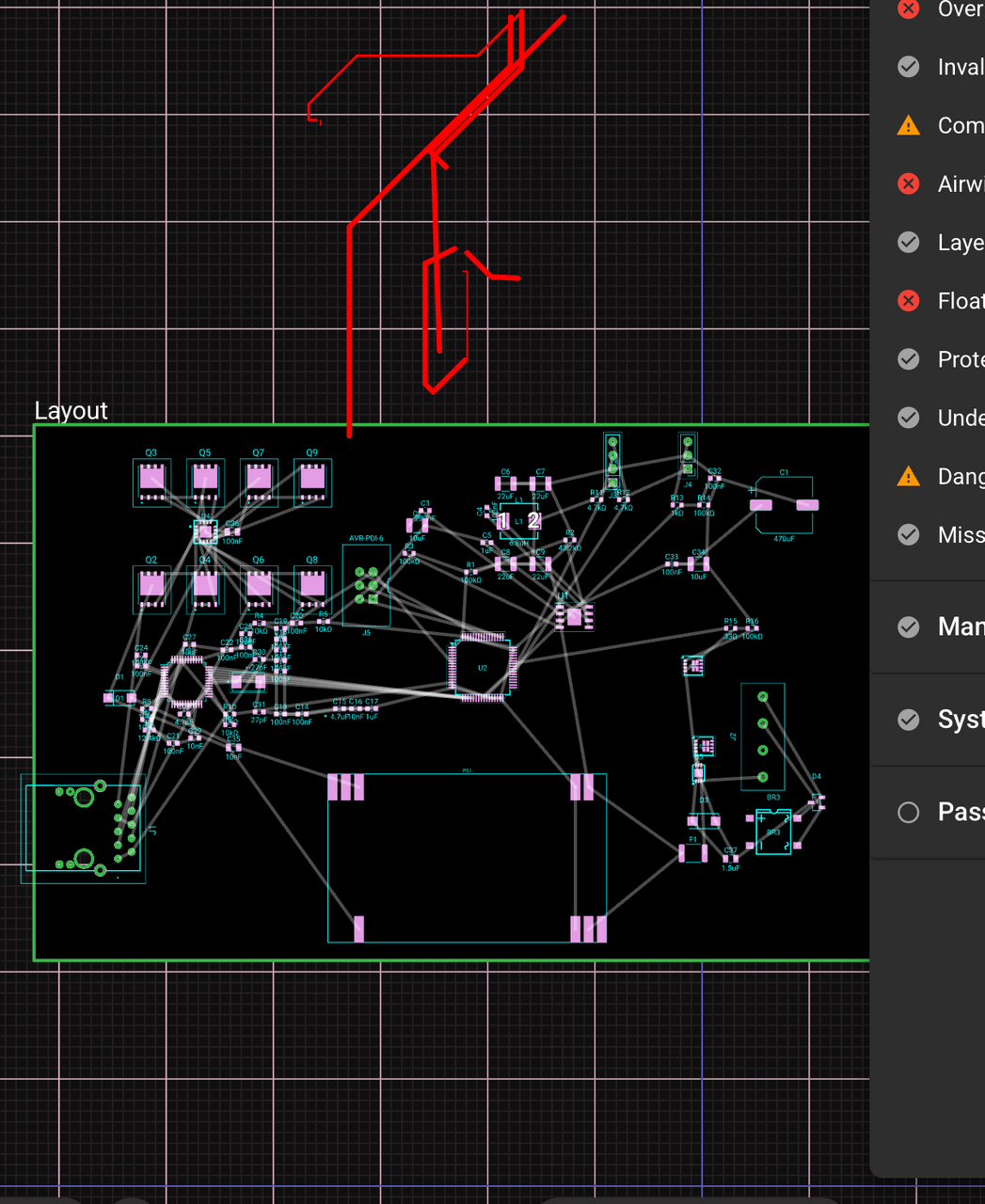
bruh you didn't even wire it together and created more issues
Image
Worked for 1 min 3 sec
You’re right. I checked history: the bad work is exactly 8 routing commits from my last pass, and they can be cleanly reverted without touching your earlier manual move or the C1/property fixes.
Safe recovery point:
- Revert to commit #bd42c4c0
- This removes only the 8 bad
mutate_layout_routeedits. - It preserves your prior layout changes and the C1 footprint/property work.
I will not do anything else unless you approve. If you want me to undo the damage, say:
Revert to #bd42c4c0
Revert bad routes
Show route diff
Revert and run DRC
Protect current state
Manual routing plan
Refine this doc
Ask about this doc
Board Bring-Up Plan — PoE Lighting Controller
Updated: 2026-07-04
Status: Prototype bring-up plan; do not treat as production release approval.
Status: Prototype bring-up plan; do not treat as production release approval.
Prerequisites
Equipment
- Digital multimeter.
- Oscilloscope with short ground spring for switching-node and ripple checks.
- Current-limited IEEE 802.3bt-capable PoE injector/switch appropriate for the AG59824-LPB power class.
- ST-LINK debugger/programmer.
- Ethernet cable and known-good Ethernet switch/router.
- Small 24V dummy load for first PWM/output test.
- Full-load 24V test load for later thermal validation.
- Thermocouples or IR camera for power-stage thermal tests.
Safety / scope notes
- The design targets PS1 AG59824-LPB, a 24V, 4A-class isolated PoE PD module with production headroom for a 2–3A lighting output.
- Do not connect a full 2–3A lighting load until basic power rails, firmware control, PWM switching, and short-duration dummy-load tests pass.
- Rev-1 output protection is intentionally limited for prototype validation. Externally powered reverse polarity, hard output short, hot-plug capacitance, and inductive kick remain production/later-revision validation items unless the protection stage is expanded.
- The PCB is not currently manufacturing-ready: latest DRC reports 319 airwires, 1 overlapping-copper error, 1 floating-copper error, and 2 dangling-trace warnings; manufacturing review reports 55 missing MPN errors.
1. Visual Inspection
Before power:
- Confirm all fitted parts match the released BOM revision.
- Confirm component orientation and pin-1 marks for U1, U2, U3, U4, U5, PS1, Q1, Q2–Q10, BR3, D1, D3, D4, and Y1.
- Confirm C1 polarity/marking if a polarized polymer/electrolytic capacitor is selected.
- Confirm J1 is the intended PoE-rated MagJack, not a non-PoE RJ45/magnetics part.
- Inspect PS1 pads and solder joints carefully; this is the central power module and footprint alignment is high risk.
- Inspect Q1 and Q10 drain/source/gate pads for shorts and correct orientation.
- Inspect U1 buck regulator, L1, C2/C3/C4/C5/C6–C9 placement and solder joints.
- Inspect fine-pitch ICs U2 and U3 for bridges.
- Confirm J2 field terminal orientation: 24V output, LED switched return, DALI+, DALI-.
- Confirm J3/J4/J5 headers are fitted only if intended by the assembly variant.
2. Pre-Power Resistance Checks
Measure resistance with the board unpowered.
Table
| Net pair | Expected result | Pass criteria |
|---|---|---|
| POE_VIN_POS to POE_VIN_NEG | No hard short | Resistance rises/settles above low-ohm short; investigate any near-0Ω reading |
| ISO_24V to ISO_GND | No hard short | No near-0Ω short; bulk capacitors may charge from meter |
| 24V_FUSED to ISO_GND | No hard short | No near-0Ω short |
| 24V_OUT to ISO_GND | No hard short | No near-0Ω short through Q1/Q10 path |
| 3V3 to ISO_GND | No hard short | No near-0Ω short; logic decoupling may charge from meter |
| BUCK_SW to ISO_GND | No hard short | May read through inductor/regulator path; compare against expected topology |
| W5500_1V2O to ISO_GND | No hard short | No near-0Ω short |
If any rail reads as a hard short, stop and inspect/rework before applying power.
3. Power Rail Verification
Table
| Rail / node | Source | Expected voltage | Measure at | Initial current/load limit | Pass criteria |
|---|---|---|---|---|---|
| POE_VIN_POS / POE_VIN_NEG | J1 + LT4321 active bridge into PS1 input | PoE rectified input, approximately 36–57V during normal PoE operation | PS1 VIN pins / D1/C35/C36 region | PSE limited | Stable after detection/classification; no repeated PSE cycling |
| ISO_24V | PS1 AG59824-LPB +VDC/−VDC output | ~24V nominal | C1/C34/C33 or U1 VIN | No external load initially | Stable, no shutdown/cycling |
| 24V_FUSED | F1 downstream of ISO_24V | ~24V | F1 output / Q10 source | No external load initially | Same as ISO_24V within fuse drop |
| 24V_OUT | Q10/U5 protected output path | ~24V | J2 24V pin to ISO_GND | Small dummy load first | Stable under small load; no Q10/U5 overheating |
| 3V3 | U1 LMR33630ADDA buck | 3.3V nominal | C6–C9, U2 VDD, U3 VDD | Logic load only | 3.135–3.465V for first-pass validation |
| BUCK_VCC | U1 internal VCC pin | Regulator internal VCC level per datasheet | C5 | Do not externally load | Present/stable after ISO_24V applied |
| W5500_1V2O | U3 internal regulator | ~1.2V | C29 | Do not externally load | Present after 3V3 and W5500 power are stable |
First power-on sequence
- Connect board to a current-limited 802.3bt-capable PoE source with no external lighting load connected.
- Verify the PSE does not repeatedly cycle.
- Measure POE_VIN_POS/POE_VIN_NEG at PS1 input.
- Measure ISO_24V at C1/C34/C33 region.
- Measure 24V_FUSED and 24V_OUT with no external load.
- Measure 3V3 at U2/U3 decoupling capacitors.
- Measure W5500_1V2O at C29.
- Check U1 switching waveform only with proper probe technique and short ground lead.
- Power down and inspect for abnormal heat before continuing.
4. Critical Signal Verification
Table
| Signal / net | Expected state | Measure at | Notes |
|---|---|---|---|
MCU reset / Net 2 | High after power-up | J5 reset pin / U2 PG10 area | Rename to MCU_NRST in a future cleanup if desired |
| MCU_BOOT0 | Low for normal flash boot | U2 PB8 / R5 | Pull-down must hold normal boot mode |
| PGOOD_3V3 | High when 3V3 is valid | U1 PG / R3 | Open-drain PG pulled to 3V3 |
| ETH_RST | High after MCU releases/reset network allows | U3 ~RST / R10 | W5500 reset should not be stuck low |
| W5500_XI / W5500_XO | 25MHz crystal oscillation | Y1 / U3 XI/XO | Probe with low capacitance only |
| SPI1_SCK/MOSI/MISO/CS | Activity during Ethernet register access | U2/U3 pins or nearby routes | Confirm with firmware transaction |
| ETH_INT | Idle high / toggles on events | U2 PA3 / U3 INT | Depends on firmware configuration |
| I2C_SCL/I2C_SDA | 3.3V idle high | J3 | R11/R12 pull-ups |
| PIR_IN | Defined low until driven | J4 / R13/R14/C32 | Verify input filter and pull-down |
| LED_PWM / MOSFET_GATE | PWM waveform after firmware command | R15 / Q1 gate | Start with dummy load only |
5. Programming and Debug Interface
Table
| Interface | Connector | Signals | Tool |
|---|---|---|---|
| STM32 SWD | J5 | 3V3, ISO_GND, SWDIO, SWCLK, NRST, optional SWO/NC | ST-LINK + STM32CubeProgrammer or OpenOCD |
Procedure:
- Verify J5 pinout against the assembly drawing before connecting ST-LINK.
- Connect ST-LINK ground to ISO_GND only.
- Confirm target voltage is ~3.3V.
- Read STM32 device ID.
- Flash a minimal board-test firmware.
- Confirm firmware can toggle a GPIO and report status over debugger/serial/logging method.
- Confirm LED_PWM output remains off by default at reset/boot.
6. Connector and Interface Tests
Table
| Connector | Function | Test method | Pass criteria |
|---|---|---|---|
| J1 | PoE RJ45 / Ethernet magnetics | PoE power-up, Ethernet link, W5500 register read | PoE negotiates, 24V rail starts, Ethernet link works |
| J2 | Field/output terminal | Continuity and controlled-load test | Correct terminal order; 24V_OUT and LED switched return behave as expected |
| J3 | I2C sensor header | Measure 3V3/GND, I2C scan with known sensor | SCL/SDA idle high; sensor detected |
| J4 | PIR header | Drive PIR input with safe 3.3V logic source | MCU reads input transition correctly |
| J5 | SWD programming | ST-LINK target detect/read ID | MCU detected reliably |
7. Functional Validation
Table
| Test | Components / nets involved | Input | Expected output | Pass criteria |
|---|---|---|---|---|
| PoE startup | J1, U4, Q2–Q9, PS1, D1/C35/C36 | 802.3bt PSE | ISO_24V ~24V | Stable startup, no repeated classification/power cycling |
| 3.3V buck | U1, L1, C2–C9, R1/R2 | ISO_24V | 3V3 | Stable voltage and acceptable ripple/thermal behavior |
| STM32 programming | U2, J5 | ST-LINK | Device ID + flash success | Reliable debug connection |
| W5500 SPI | U2, U3, Y1, SPI nets | Firmware register read | VERSIONR returns expected W5500 value | SPI transaction succeeds repeatedly |
| Ethernet link | J1, U3 | Ethernet cable/switch | Link status in W5500 | Link detected and traffic possible |
| I2C header | U2, J3, R11/R12 | Known I2C sensor | Sensor address detected | Bus scan succeeds |
| PIR input | U2, J4, R13/R14/C32 | Safe 3.3V logic stimulus | MCU input changes | Debounced/filtered state matches stimulus |
| PWM dimming, low load | U2, R15/R16, Q1, J2 | Small 24V dummy load | Controlled PWM current path | MOSFET switches, no abnormal heating |
| Protected output | U5, Q10, F1, D3, C37, J2 | Small dummy load | 24V_OUT stable | No reverse/backfeed anomaly in controlled test |
| Full-load thermal | PS1, U1, Q1/Q10, F1, copper | 24V load up to target current | Stable operation | Temperatures within selected component/enclosure limits |
8. Thermal / Full-Load Validation
Do not skip this for a 2–3A 24V lighting controller.
- Run no-load PoE startup and record temperatures after 5 minutes.
- Run light logic load only and record PS1, U1, Q1, Q10, F1, Q2–Q9 temperatures.
- Run a small 24V dummy load and verify PWM behavior.
- Increase load in steps toward target current.
- At each step, record ISO_24V, 24V_OUT, 3V3, PSE input power/class if available, PS1 case temperature, Q1/Q10/F1 temperature, and U1/L1 temperature.
- Hold target full load long enough to reach thermal steady state.
- Repeat at elevated ambient or worst-case enclosure condition before production release.
9. Known Bring-Up / Release Risks
- Current PCB DRC is not clean: 319 airwires, 1 overlapping-copper error, 1 floating-copper error, and 2 dangling-trace warnings remain.
- BOM still has 55 missing MPNs.
- PS1 footprint has been corrected at instance level, but reusable footprint/STEP validation remains a release blocker.
- J1 availability is weak in authorized channels; do not assume a replacement is drop-in.
- U2 needs exact orderable ST MPN selection.
- Q1/Q10 need exact purchasable DMT6008LFG packaging suffix and distributor source.
- U1 footprint/package should be checked against TI DDA/SO PowerPAD land pattern because the schematic package property appears suspicious.
- C1 is currently a generic capacitor entry with polymer/electrolytic role; exact polarized part, footprint, height, ripple current, and polarity marking must be locked.
- Rev-1 output protection is not a complete industrial eFuse/hot-swap/inductive-load protection solution.
- DALI is treated as protected terminal/placeholder scope unless a dedicated DALI interface is added and validated.
Pass / Fail Summary
Table
| Test section | Result | Notes |
|---|---|---|
| Visual inspection | [ ] Pass / [ ] Fail | |
| Pre-power resistance | [ ] Pass / [ ] Fail | |
| PoE startup | [ ] Pass / [ ] Fail | |
| Power rails | [ ] Pass / [ ] Fail | |
| Programming | [ ] Pass / [ ] Fail | |
| Ethernet/W5500 | [ ] Pass / [ ] Fail | |
| I2C/PIR headers | [ ] Pass / [ ] Fail | |
| PWM/output dummy load | [ ] Pass / [ ] Fail | |
| Full-load thermal | [ ] Pass / [ ] Fail |
Board status: [ ] Ready for next test / [ ] Requires rework / [ ] Stop — unsafe or release-blocking issue
Prerequisites
Equipment
Safety / scope notes
1. Visual Inspection
2. Pre-Power Resistance Checks
3. Power Rail Verification
First power-on sequence
4. Critical Signal Verification
5. Programming and Debug Interface
6. Connector and Interface Tests
7. Functional Validation
8. Thermal / Full-Load Validation
9. Known Bring-Up / Release Risks
Pass / Fail Summary
