Manufacturing Design Checklist

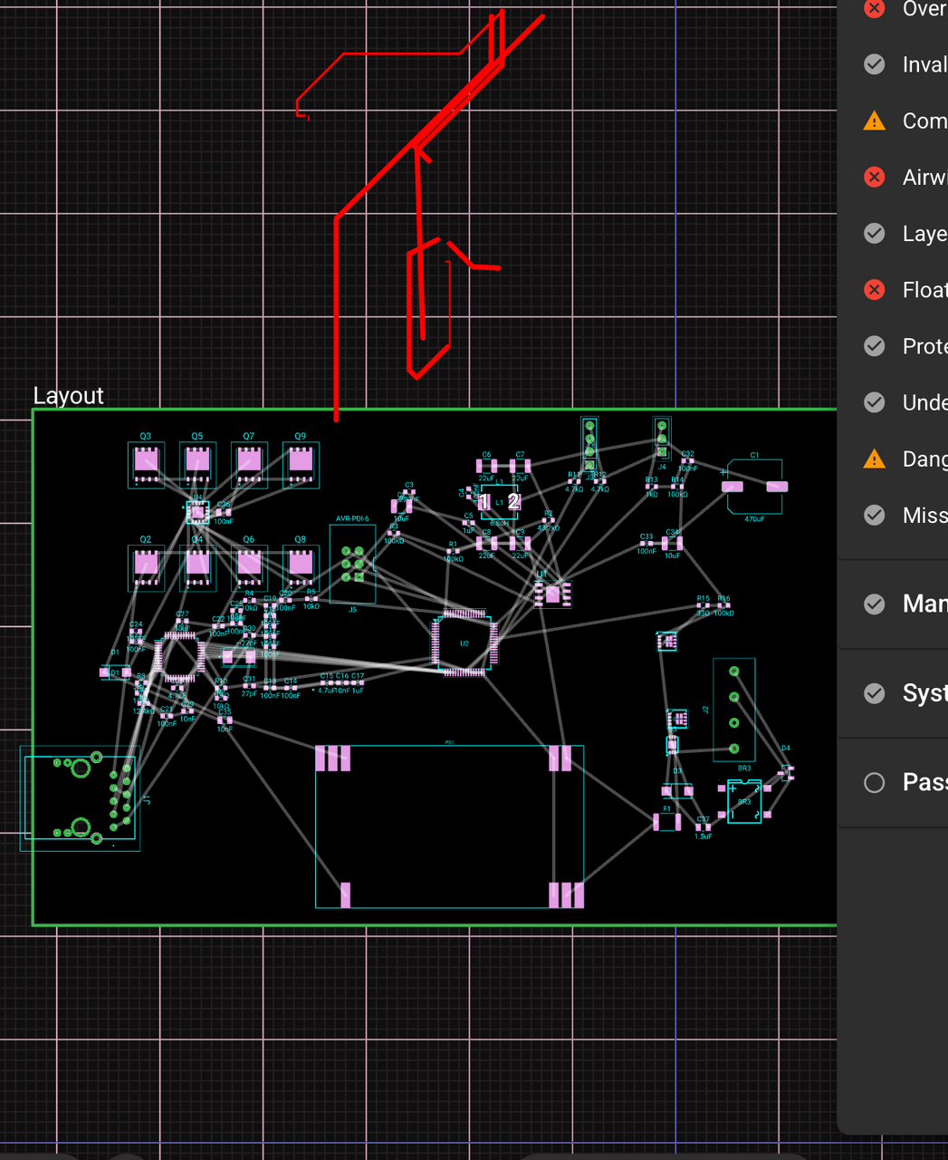
bruh you didn't even wire it together and created more issues
Screenshot 2026-07-04 at 4.41.38 PM.png

Image

You’re right. I checked history: the bad work is exactly 8 routing commits from my last pass, and they can be cleanly reverted without touching your earlier manual move or the C1/property fixes.
Safe recovery point:
  • Revert to commit #bd42c4c0
  • This removes only the 8 bad mutate_layout_route edits.
  • It preserves your prior layout changes and the C1 footprint/property work.
I will not do anything else unless you approve. If you want me to undo the damage, say:
Revert to #bd42c4c0
Revert bad routes
Show route diff
Revert and run DRC
Protect current state
Manual routing plan
J2
Q3
Q4
Q7
U5
Q5
Q2
Q9
Q8
U3
PS1
Q6
U5 IN - U5 SOURCE
BR1 + - BR2 +
BR1 + - BR2 +
R13 P2 - R14 P1
PS1 0V1_1 - PS1 0V1_2
U2 PA8 - R15 P1
BR3 AC - D4 1
U4 IN45 - Q6 S_1
Q4 S_3 - Q5 D_1
U2 PB8 - R5 P1
PS1 0V1_1 - PS1 0V1_2
U3 ~RST - R10 P2
BR1 + - BR2 +
PS1 OUT1_1 - PS1 OUT1_2
U2 VDD - C10 P1
Q3 S_3 - Q5 S_1
U2 VDD - C10 P1
PS1 0V1_1 - PS1 0V1_2
U2 PA5 - U3 SCLK
U3 PMODE0 - R9 P2
R1 P2 - R2 P1
U2 VDD - C10 P1
U4 TG36 - Q4 G
PS1 0V1_1 - PS1 0V1_2
U4 ~EN~ - Q2 D_1
PS1 OUT1_1 - PS1 OUT1_2
Q2 S_3 - Q3 D_1
PS1 0V1_1 - PS1 0V1_2
Q2 D_5 - Q4 D_1
U2 VDD - C10 P1
PS1 OUT1_1 - PS1 OUT1_2
PS1 0V1_1 - PS1 0V1_2
Q7 S_3 - Q9 S_1
U4 OUTN - Q3 S_1
U2 PA7 - U3 MOSI
U3 XO - Y1 P2
Q6 D_5 - Q8 D_1
R15 P2 - R16 P1
U2 PA6 - U3 MISO
U3 TOCAP - C28 P1
U5 GATE - Q10 G
U3 RXN - J1 RD-
PS1 0V1_1 - PS1 0V1_2
U2 PC7 - J3 SDA
U4 BG78 - Q9 G
U3 TOCAP - C28 P1
U2 VDD - C10 P1
U5 OUT - Q10 D
PS1 0V1_1 - PS1 0V1_2
Q2 S_3 - Q3 D_1
U2 VDD - C10 P1
R15 P2 - R16 P1
PS1 0V1_1 - PS1 0V1_2
U3 ~RST - R10 P2
PS1 0V1_1 - PS1 0V1_2
J5 Pin_4 - U2 PA14
U4 TG45 - Q6 G
U2 VDD - C10 P1
J1 VC+_2 - BR2 AC
U4 BG45 - Q7 G
U4 IN78 - Q8 S_1
BR3 AC - D4 2
J2 ~ - Q1 D
U3 PMODE2 - R7 P2
PS1 0V1_1 - PS1 0V1_2
U2 VDD - C10 P1
PS1 OUT1_1 - PS1 OUT1_2
U3 XI/CLKIN - Y1 P1
U5 GATE - Q10 G
U3 ~RST - R10 P2
PS1 0V1_1 - PS1 0V1_2
U4 BG36 - Q5 G
BR1 - - BR2 -
PS1 0V1_1 - PS1 0V1_2
J1 RCT - BR1 AC
U2 PC7 - J3 SDA
U2 VDD - C10 P1
U1 BOOT - C4 P1
F1 P2 - D2 A
U4 TG45 - Q6 G
U2 VDD - C10 P1
U2 VDD - C10 P1
U2 VDD - C10 P1
BR3 AC - D4 2
R15 P2 - R16 P1
U4 OUTP - U4 EN
U2 VDD - C10 P1
J5 Pin_4 - U2 PA14
PS1 0V1_1 - PS1 0V1_2
Q8 S_3 - Q9 D_1
U2 VDD - C10 P1
U2 PA3 - U3 ~INT
U2 VDD - C10 P1
U1 PG - R3 P1
PS1 0V1_1 - PS1 0V1_2
R1 P2 - R2 P1
U2 VDD - C10 P1
U2 VDD - C10 P1
U2 VDD - C10 P1
U4 TG12 - Q2 G
J5 Pin_5 - U2 PG10
U3 XO - Y1 P2
U4 BG78 - Q9 G
J5 Pin_2 - U2 PA13
R6 P2 - U3 RSVD
PS1 0V1_1 - PS1 0V1_2
Q5 S_3 - Q7 S_1
PS1 0V1_1 - PS1 0V1_2
U1 SW - C4 P2
J5 Pin_5 - U2 PG10
U3 TXP - J1 TD+
U3 PMODE1 - R8 P2
U2 VDD - C10 P1
U2 VDD - C10 P1
U1 EN - C2 P1
PS1 0V1_1 - PS1 0V1_2
U2 VDD - C10 P1
U2 VDD - C10 P1
J1 VC-_2 - BR2 AC
J1 VC-_2 - BR2 AC
U3 1V2O - C29 P1
J4 Pin_3 - R13 P1
U2 VDD - C10 P1
PS1 0V1_1 - PS1 0V1_2
U3 PMODE0 - R9 P2
U3 TXP - J1 TD+
PS1 OUT1_1 - PS1 OUT1_2
U3 RXN - J1 RD-
Q4 S_3 - Q5 D_1
R6 P2 - U3 RSVD
U2 VDD - C10 P1
BR1 - - BR2 -
U4 BG45 - Q7 G
U2 VDD - C10 P1
J5 Pin_5 - U2 PG10
U3 RXP - J1 RD+
U2 VDD - C10 P1
Q5 S_3 - Q7 S_1
U4 TG78 - Q8 G
U2 VDD - C10 P1
BR1 + - BR2 +
J1 VC+_2 - BR2 AC
F1 P2 - D2 A
BR3 AC - D4 2
U2 PA3 - U3 ~INT
PS1 0V1_1 - PS1 0V1_2
Q3 S_3 - Q5 S_1
U3 EXRES1 - R6 P1
U3 1V2O - C29 P1
PS1 0V1_1 - PS1 0V1_2
U1 VCC - C5 P1
U4 TG36 - Q4 G
U5 OUT - Q10 D
U2 PA7 - U3 MOSI
U3 PMODE1 - R8 P2
PS1 0V1_1 - PS1 0V1_2
U2 VDD - C10 P1
U2 VDD - C10 P1
U5 IN - U5 SOURCE
U2 VDD - C10 P1
U4 TG78 - Q8 G
BR3 AC - D4 1
PS1 0V1_1 - PS1 0V1_2
U4 IN45 - Q6 S_1
U4 IN36 - Q4 S_1
U2 PA8 - R15 P1
Q4 D_5 - Q6 D_1
R13 P2 - R14 P1
PS1 0V1_1 - PS1 0V1_2
U2 VDD - C10 P1
PS1 0V1_1 - PS1 0V1_2
U2 VDD - C10 P1
Q7 S_3 - Q9 S_1
U5 OUT - Q10 D
U2 PA4 - U3 ~SCS
U4 ~EN~ - Q2 D_1
U5 IN - U5 SOURCE
U1 BOOT - C4 P1
U5 IN - U5 SOURCE
J4 Pin_3 - R13 P1
BR1 + - BR2 +
PS1 0V1_1 - PS1 0V1_2
U4 BG12 - Q3 G
U1 SW - C4 P2
U3 RXP - J1 RD+
PS1 0V1_1 - PS1 0V1_2
U1 VCC - C5 P1
U2 PC6 - J3 SCL
PS1 0V1_1 - PS1 0V1_2
U4 IN78 - Q8 S_1
Q8 S_3 - Q9 D_1
U1 EN - C2 P1
J2 ~ - Q1 D
U2 VDD - C10 P1
J5 Pin_6 - U2 PB3
PS1 0V1_1 - PS1 0V1_2
Q6 S_3 - Q7 D_1
U2 VDD - C10 P1
U4 OUTP - U4 EN
PS1 0V1_1 - PS1 0V1_2
U2 VDD - C10 P1
U5 OUT - Q10 D
Q6 S_3 - Q7 D_1
U2 VDD - C10 P1
U4 OUTN - Q3 S_1
J1 TCT - BR1 AC
U1 SW - C4 P2
U2 VDD - C10 P1
PS1 0V1_1 - PS1 0V1_2
BR1 - - BR2 -
U2 VDD - C10 P1
U2 PB8 - R5 P1
U2 VDD - C10 P1
PS1 0V1_1 - PS1 0V1_2
U3 XI/CLKIN - Y1 P1
U1 PG - R3 P1
U2 PC6 - J3 SCL
BR1 - - BR2 -
BR1 - - BR2 -
PS1 0V1_1 - PS1 0V1_2
U2 PC6 - J3 SCL
PS1 0V1_1 - PS1 0V1_2
U2 PA5 - U3 SCLK
J5 Pin_2 - U2 PA13
PS1 0V1_1 - PS1 0V1_2
U2 VDD - C10 P1
U3 XI/CLKIN - Y1 P1
PS1 0V1_1 - PS1 0V1_2
J5 Pin_5 - U2 PG10
PS1 0V1_1 - PS1 0V1_2
U4 IN12 - Q2 S_1
U4 BG36 - Q5 G
J5 Pin_6 - U2 PB3
U2 VDD - C10 P1
U3 XO - Y1 P2
U2 PC7 - J3 SDA
PS1 0V1_1 - PS1 0V1_2
BR3 AC - D4 1
R13 P2 - R14 P1
R1 P2 - R2 P1
PS1 0V1_1 - PS1 0V1_2
U2 VDD - C10 P1
R13 P2 - R14 P1
Q6 D_5 - Q8 D_1
U4 IN12 - Q2 S_1
U2 VDD - C10 P1
U2 VDD - C10 P1
U2 PA6 - U3 MISO
U4 BG12 - Q3 G
U2 PA4 - U3 ~SCS
PS1 0V1_1 - PS1 0V1_2
U3 PMODE2 - R7 P2
U2 VDD - C10 P1
U5 OUT - Q10 D
Q2 D_5 - Q4 D_1
U3 TXN - J1 TD-
PS1 0V1_1 - PS1 0V1_2
Q4 D_5 - Q6 D_1
U2 VDD - C10 P1
U4 TG12 - Q2 G
J1 RCT - BR1 AC
J1 TCT - BR1 AC
U3 EXRES1 - R6 P1
PS1 0V1_1 - PS1 0V1_2
U2 VDD - C10 P1
PS1 OUT1_1 - PS1 OUT1_2
U3 TXN - J1 TD-
U1 EN - C2 P1
U4 IN36 - Q4 S_1
U2 VDD - C10 P1
R15
Resistance
33Ω
C6
End of Life
Capacitance
22uF
R11
Resistance
4.7kΩ
R16
Resistance
100kΩ
C7
End of Life
Capacitance
22uF
C28
Capacitance
4.7uF
C12
Capacitance
100nF
C10
Capacitance
100nF
C35
Capacitance
10nF
C2
Capacitance
10uF
C5
Capacitance
1uF
C19
Capacitance
1uF
C15
Capacitance
4.7uF
C3
Capacitance
220nF
R14
Resistance
100kΩ
C27
Capacitance
10uF
C18
Capacitance
100nF
R3
Resistance
100kΩ
C11
Capacitance
100nF
R12
Resistance
4.7kΩ
C20
Capacitance
100nF
R2
Resistance
43.2kΩ
R4
Resistance
10kΩ
C31
Not Recommended for New Designs
Capacitance
27pF
C26
Capacitance
100nF
R1
Resistance
100kΩ
C17
Capacitance
1uF
C22
Capacitance
100nF
C29
Capacitance
10nF
C37
Capacitance
1.5uF
C14
Capacitance
100nF
C36
Capacitance
100nF
C1
Capacitance
470uF
C34
Capacitance
10uF
C13
Capacitance
100nF
C30
Not Recommended for New Designs
Capacitance
27pF
R9
Resistance
10kΩ
R6
Resistance
12.4kΩ
C8
End of Life
Capacitance
22uF
R5
Resistance
10kΩ
R10
Resistance
10kΩ
C9
End of Life
Capacitance
22uF
C25
Capacitance
100nF
C24
Capacitance
100nF
R13
Resistance
1kΩ
C32
Capacitance
100nF
C4
Capacitance
100nF
C16
Capacitance
10nF
C23
Capacitance
100nF
R7
Resistance
10kΩ
C21
Capacitance
100nF
R8
Resistance
10kΩ
C33
Capacitance
100nF
U4
BR3
U1
L1
Inductance
6.8uH
F1
D4
U2
J5
D1
J3
Y1
J1
Q10
J4
D3
Q1

Refine this doc
Ask about this doc
PCB Pre-Layout Gate — Power Stage
Status
Power-first PCB placement is not yet release-ready, but the previous AG59824-LPB pad-footprint blocker has been partially remediated from public Silvertel land-pattern data. The AG59824-LPB layout instance now uses the datasheet-derived 5.00mm x 1.83mm SMD pads, 26.57mm row spacing, 45.31mm group spacing, and 51.6mm x 31.0mm package size. A proper reusable part footprint/STEP association is still preferred before manufacturing release.
Footprint / Land Pattern Verification

Table


Part / BlockCurrent statusEvidence / issueAction before routing
LT4321IUF#PBF U4Acceptable footprint familyDatasheet: 16-QFN 4mm x 4mm, 0.65mm pitch, exposed OUTN pad. Current layout footprint uses 16 QFN-style pads plus exposed OUTN pad and matches expected package class.Verify pin-1 orientation during placement; keep OUTP/OUTN bypass C36 close.
BSC040N10NS5ATMA1 Q2-Q9Acceptable footprint familyDatasheet: PG-TDSON-8 / SuperSO8, source pins 1-3, gate pin 4, drain pins 5-8 plus exposed drain pad. Current footprint has source, gate, drain fingers and exposed drain pad style.Use large copper on drain/source pads and thermal vias/planes; use direct-connect for power copper.
DMT6008LFG Q1/Q10Acceptable footprint familyPowerDI3333-8 library footprint available and already used in schematic.Add copper pour/thermal spreading for Q1 load switch and Q10 ideal-diode path.
LTC4359CDCB U5Acceptable footprint family with caveatDatasheet: 6-DFN 2mm x 3mm. Exposed pad optional VSS; datasheet warns DFN pin spacing may be a concern above 30V and suggests leaving exposed pad open if creepage is a concern. Current schematic connects EP to ISO_GND.Before release, review creepage/clearance for 24V field conditions; consider EP-open variant if contamination/clearance risk dominates.
AG59824-LPB PS1Partially remediated; still needs release verificationDatasheet package is about 51.6mm x 31.0mm max; land pattern pad span is about 45.31mm x 26.57mm with 5.00mm x 1.83mm pads. The generated pad geometry was corrected in the PCB instance from Figure 17 dimensions. The official Silvertel Ag59800 STEP ZIP was added as a project asset.Before manufacturing release, verify pin-1 orientation against the Silvertel drawing and replace the instance-level fix with a proper reusable AG59824-LPB footprint/STEP asset if possible.
J2 691241710004 terminal blockElectrically suitableDatasheet: 5.00mm pitch, 4 positions, 14A rating, 300VAC UL / 250VAC VDE, 30–14AWG.Good for 3A rail; keep at board edge and provide strain/clearance.
Installer-Abuse Case Decision
For the current schematic, output protection is designed primarily for:
  1. Reversed passive load wiring at the 24V output terminal.
  2. Reverse current/backfeed blocking into the board from the output side.
It is not yet fully validated as a complete industrial eFuse/hot-swap solution for every abuse case, especially:
  • an external powered 24V supply connected backwards,
  • shorted output cable at full PoE power,
  • hot-plug into large downstream capacitance,
  • inductive load energy without a defined clamp path.
If those are expected installer conditions, add a dedicated eFuse/hot-swap/load-switch protection stage or expand the LTC4359 protection network per datasheet Figure 14.
3A Copper / Thermal Constraints Applied
The following layout net rules were applied:

Table


NetRule applied
ISO_24VminTraceWidth = 2.0mm
24V_FUSEDminTraceWidth = 2.0mm
24V_OUTminTraceWidth = 2.0mm
LED_SW_RETURNminTraceWidth = 2.0mm
POE_VIN_POSminTraceWidth = 1.0mm
POE_VIN_NEGminTraceWidth = 1.0mm
3V3minTraceWidth = 0.5mm
Additional layout setup completed:
  • 4-layer board stackup retained.
  • Mid-Layer 1 assigned as Ground Plane.
  • Mid-Layer 2 assigned as Power Plane.
  • Ethernet TX/RX nets tagged as 100 ohm differential controlled-impedance pairs.
These are conservative pre-routing minimums. Preferred production routing is copper pours/planes for 24V and return paths, not long narrow traces.
Thermal / Placement Requirements Before Power-First Layout
  • Use 4-layer board stackup with a solid ground reference plane and power copper plane/regions.
  • Place RJ45, LT4321 active bridge, input TVS, and AG59824-LPB close together, with PoE high-voltage/current paths short and wide.
  • Place AG59824-LPB so its thermal-interface region can couple to copper and, ideally, enclosure/gap pad.
  • Place 24V output terminal J2 at board edge.
  • Place F1, Q10/U5, D3 TVS, and J2 as a tight protected-output chain.
  • Place U1 buck and its VIN/SW loop parts away from Ethernet magnetics and MCU crystal areas.
  • Use thermal via arrays under/near SuperSO8/PowerDI drain/source copper regions where heat must spread to inner/bottom planes.
Current Decision Gates Before Continuing to Schematic Changes
  1. CLOSED for rev 1: DALI is a protected-terminal placeholder only. Reserve MCU pins and bring DALI+ / DALI- to the terminal block; do not add the full DALI interface circuit on rev 1.
  2. CLOSED for rev 1: output protection target is reversed passive load protection only. Externally powered reverse polarity, shorted cable, hot-plug capacitance, and inductive kick are documented rev-2/production concerns.
  3. CLOSED: do not proceed to placement using only the corrected instance-level AG59824 pad geometry. Stop until AG59824-LPB has a correct reusable footprint/STEP association.
Rev-1 Scope Decisions From User Note
  • DALI: placeholder/protected terminal only for this revision.
  • 24V output abuse: reversed passive load protection only for first prototype.
  • AG59824-LPB footprint: must be correct before placement because it is the critical/expensive power module.
  • Status

  • Footprint / Land Pattern Verification

  • Installer-Abuse Case Decision

  • 3A Copper / Thermal Constraints Applied

  • Thermal / Placement Requirements Before Power-First Layout

  • Current Decision Gates Before Continuing to Schematic Changes

  • Rev-1 Scope Decisions From User Note

Assets

PS1 Silvertel AG59800/AG59824-LPB detailed STEP model

PS1 Silvertel AG59800/AG59824-LPB detailed STEP model

Ag59800_Detailed.step3D Model
Silvertel Ag59800 simplified STEP model

Silvertel Ag59800 simplified STEP model

Ag59800_Simplified.step3D Model
kicad_mod

J1 Abracon ARJM11D7-114-AB-EW2 reference KiCad footprint

ARJM11D7-114-AB-EW2.kicad_modFootprint
Silvertel Ag59800 detailed STEP model

Silvertel Ag59800 detailed STEP model

Ag59800_Detailed.step3D Model
step

Silvertel Ag59800/AG59824-LPB STEP package

Ag59800.zip3D Model

PoE Lighting Controller

PoE Lighting Controller thumbnail
Integrated PoE lighting-control PCB with 802.3bt PoE input, isolated 24V/3.3V power, Ethernet control, MOSFET dimming, DALI interface, and sensor inputs.

Properties

Lighting

24

V

Ethernet

PoE

Pricing & Availability

Distributor

Qty 1

Arrow

$29.78–$55.45

Digi-Key

$19.37–$20.44

HQonline

$7.45–$7.49

LCSC

$34.10–$35.63

Mouser

$68.08–$68.31

TME

$12.22–$12.26

Verical

$27.94–$277.41

Controls