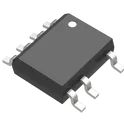
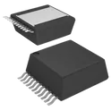
LM1117DT-ADJ/NOPB
Adjustable Low-Dropout (LDO) Linear Voltage Regulator – Positive adjustable LDO voltage regulator designed for power supplies, industrial control systems, embedded electronics, consumer devices, communication equipment, and analog circuits. Delivers up to 800 mA output current with an adjustable output voltage range of 1.25 V to 13.8 V using an external resistor divider. Operates from an input voltage up to 15 V with a maximum dropout voltage of 1.2 V at 800 mA, making it suitable for low-dropout linear regulation. Features 1% output voltage accuracy, 75 dB PSRR (120 Hz), 5 mA typical quiescent current, current limiting, and thermal shutdown protection for reliable operation. Designed for surface-mount applications in a TO-252-3 (DPAK) package and operates over a 0°C to +125°C temperature range. #TexasInstruments #LM1117DTADJNOPB #LM1117 #LDO #LinearRegulator #VoltageRegulator #AdjustableRegulator #PowerManagement #DPAK #EmbeddedSystems... show more0 Uses
0 Stars

TPS5405
12V to fixed 5V 2A Non-Synchronous Step-Down Regulator. The TPS5405 is a monolithic non-synchronous buck regulator with wide operating input voltage range from 6.5 V to 28 V. Current mode control with internal slope compensation is implemented to reduce component count. TPS5405 also features a light load pulse skipping mode, which allows for a power loss reduction from the input power supply to the system at light loading. The switching frequency of the converters can be set from 50 kHz to 1.1 MHz with an external resistor. Frequency spread spectrum operation is introduced for EMI reduction. LX anti-ringing is added to address high frequency EMI issues. A cycle-by-cycle current limit with frequency fold back protects the IC at over loading condition.... show more160 Uses
0 Stars
TPS259531DSGT
IC SURGE STOPPER 2.7V~18V WSON-8-EP(2x2) The TPS2595xx family of eFuses (integrated FET hot swap devices) is a highly integrated circuit protection and power management solution in a small package. The devices provide multiple protection modes using very few external components and are a robust defense against overloads, short circuits, voltage surges, and excessive inrush current. Output current limit level can be set with a single external resistor. It is also possible to get an accurate sense of the output load current by measuring the voltage drop across the current limit resistor. Applications with particular inrush current requirements can set the output slew rate with a single external capacitor. Overvoltage events are quickly limited by internal clamping circuits to a safe fixed maximum, with no external components required. The TPS259573 variant provides an option to set a user-defined overvoltage cutoff threshold. Quick output discharge function can be implemented in the TPS2595x5 variants by connecting the OUT pin to the QOD pin. The devices are characterized for operation over the temperature range of –40°C to +125°C. 1• Wide Input Voltage Range: 2.7 V to 18 V – 20 V Absolute Maximum – 3 V to 18 V for TPS2595x5 Version • Low On-Resistance: RON = 34 mΩ (Typical) • Fast Overvoltage Protection Clamp (3.8-V, 5.7-V, and 13.7-V options) With a Response Time of 5 µs (Typical) • TPS2595x0, TPS2595x1, TPS2595x5: Active High Enable Input With Adjustable Undervoltage Lockout (UVLO) • TPS2595x3: Active Low Enable Input With Adjustable Overvoltage Lockout (OVLO) • Adjustable Current Limit With Load Current Monitor Output (ILM) – Current Range: 0.5 A to 4 A – Current Limit Accuracy: ±7.5% • Adjustable Output Slew Rate Control (dVdt) • Over Temperature Protection (OTP) • Fault Indication Pin (FLT ) • UL 2367 Recognition – File No. E169910 – RILM >= 487 Ω (4.42 A maximum) • IEC 62368-1 Certified • Safe During Single Point Failure Test (IEC 62368- 1) – ILM Pin Open/Short Detection #CommonPartsLibrary #IntegratedCircuit #PowerManagement... show more166 Uses
0 Stars
SRG0630-100-M
SRG0630-100-M is a JIERR 10 µH ±20% magnetically shielded high-current SMD power inductor with 68 mΩ max DCR, 5.0 A saturation current, 4.5 A heating current, and a 7.4 × 6.6 × 3.0 mm package. Keywords: SRG0630-100-M, 10uH power inductor, 5A shielded inductor, 0630 SMD inductor, high-current inductorFRQ1206J1R0 TS is a FOJAN 1 Ω ±5% thick-film chip resistor rated for 250 mW in a 1206 surface-mount package. Keywords: FRQ1206J1R0 TS, 1Ω resistor, 1206 resistor, 5% tolerance, 250mW SMD... show more4 Uses
0 Stars

BQ25173
The BQ25173 is an integrated 800-mA linear charger for 1- to 4-cell supercapacitors. Features • Input voltage up-to 40-V tolerant • Automatic Sleep mode for low power consumption – 350-nA leakage current – 2-µA input leakage current when charge disabled • Supports 1- to 4-cell supercapacitor • Supports charging supercapacitor from 0 V • External resistor programmable operation – FB pin to adjust supercapacitor regulation voltage – ISET to set charge current from 10 mA to 800 mA • High accuracy – ±1% charge voltage accuracy – ±10% charge current accuracy • Charging features – CE pin for charging function control – Open-drain output for status and fault indication – Open-drain output for power-good indication • Integrated fault protection – 18-V IN overvoltage protection – 1000-mA overcurrent protection – 125°C thermal regulation; 150°C thermal shutdown protection – OUT short-circuit protection – ISET pin short/open protection WSON-8 2.0mmx2.0mm... show more24 Uses
0 Stars
TPS62840DLCR
1.8V to 6.5V, 750mA, 60nA IQ step-down converter The TPS62840 is a high-efficiency step-down converter with ultra-low operating quiescent current of typically 60 nA. The device contains special circuitry to achieve just 120 nA IQ in 100% mode to further extend battery life near the end of discharge. The device uses DCS-Control to cleanly power radios and operates with a typical switching frequency of 1.8 MHz. In Power-Save Mode, the device extends the light load efficiency down to a load current range of 1 μA and below. 16 predefined output voltages can be selected by connecting a resistor to pin VSET, making the device flexible for various applications with a minimum amount of external components. The STOP pin of the device immediately eliminates any switching noise in order to take a noise-free measurement in test and measurement systems. The TPS62840 provides an output current of up to 750 mA. With an input voltage of 1.8 V to 6.5 V, the device supports multiple power sources such as 2S to 4S Alkaline, 1S to 2S Li-MnO2 , or 1S Li-Ion/LiSOCl2 • 60-nA operating quiescent current • 100% duty-cycle mode with 120-nA IQ • Input voltage range VIN from 1.8 V to 6.5 V • Output current up to 750 mA • RF friendly DCS-Control™ • 80% efficiency at 1 µA IOUT (3.6 VIN to 1.8 VOUT) • 16 selectable output voltages via VSET pin • Auto transition PFM/PWM or forced-PWM mode • Selectable forced PWM and STOP modes • Output discharge function • 25-nA shutdown current • SON-8, WCSP-6 and thermally enhanced HVSSOP-8 packages #CommonPartsLibrary #IntegratedCircuit #PowerManagement... show more303 Uses
0 Stars
INA228AIDGSR
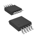
Power Supply Controller Digital Power Monitor 10-VSSOP The INA228 is an ultra-precise digital power monitor with a 20-bit delta-sigma ADC specifically designed for current-sensing applications. The device can measure a full-scale differential input of ±163.84 mV or ±40.96 mV across a resistive shunt sense element with common-mode voltage support from –0.3 V to +85 V. The INA228 reports current, bus voltage, temperature, power, energy and charge accumulation while employing a precision ±0.5% integrated oscillator, all while performing the needed calculations in the background. The integrated temperature sensor is ±1°C accurate for die temperature measurement and is useful in monitoring the system ambient temperature. The low offset and gain drift design of the INA228 allows the device to be used in precise systems that do not undergo multi-temperature calibration during manufacturing. Further, the very low offset voltage and noise allow for use in mA to kA sensing applications and provide a wide dynamic range without significant power dissipation losses on the sensing shunt element. The low input bias current of the device permits the use of larger currentsense resistors, thus providing accurate current measurements in the micro-amp range. The device allows for selectable ADC conversion times from 50 µs to 4.12 ms as well as sample averaging from 1x to 1024x, which further helps reduce the noise of the measured data. • High-resolution, 20-bit delta-sigma ADC • Current monitoring accuracy: – Offset voltage: ±1 µV (maximum) – Offset drift: ±0.01 µV/°C (maximum) – Gain error: ±0.05% (maximum) – Gain error drift: ±20 ppm/°C (maximum) – Common mode rejection: 154 dB (minimum) • Power monitoring accuracy: – 0.5% full scale, –40°C to +125°C (maximum) • Energy and charge accuracy: – 1.0% full scale (maximum) • Fast alert response: 75 μs • Wide common-mode range: –0.3 V to +85 V • Bus voltage sense input: 0 V to 85 V • Shunt full-scale differential range: ±163.84 mV / ±40.96 mV • Input bias current: 2.5 nA (maximum) • Temperature sensor: ±1°C (maximum at 25°C) • Programmable resistor temperature compensation • Programmable conversion time and averaging • 2.94-MHz high-speed I2C interface with 16 pinselectable addresses • Operates from a 2.7-V to 5.5-V supply: – Operational current: 640 µA (typical) – Shutdown current: 5 µA (maximum) #CommonPartsLibrary #IntegratedCircuit #PowerManagement... show more225 Uses
0 Stars
RC0603FR-075K1L
5.1 kOhms ±1% 0.1W, 1/10W Chip Resistor 0603 (1608 Metric) Moisture Resistant Thick Film Chip Resistor providing a fixed 5.1 kΩ resistance for general-purpose circuit applications. This RC0603 thick-film resistor features a 0603 (1608 Metric) package, ±1% resistance tolerance, 0.1 W (1/10 W) power rating, and a ±100 ppm/°C temperature coefficient, making it suitable for precision signal conditioning, biasing, and current-limiting circuits. #ChipResistor #ThickFilmResistor #0603 #5.1kOhm #0.1W #1Percent #100ppm #YAGEO... show more184 Uses
0 Stars
MFR-25FBF52-68K
Metal film resistor providing 68 kΩ resistance with ±1% tolerance and 0.25 W (1/4 W) power rating for general-purpose and power applications. It features a ±100 ppm/°C temperature coefficient, 250 V maximum working voltage, and -55°C to +155°C operating temperature range in an axial through-hole package. #MetalFilmResistor #ThroughHole #68kOhm #YAGEO... show more0 Uses
0 Stars
BC847
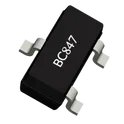
All details fully confirmed across multiple authoritative sources including Nexperia, ROHM, Farnell, and others. Here's the complete spec. Engineering Specification — BC847 Device Type: NPN General-Purpose Bipolar Junction Transistor Multiple Manufacturers: Nexperia (formerly Philips/NXP), ROHM, Infineon, Diotec, Vishay, ON Semiconductor, and others General Description The BC847 is an NPN general-purpose silicon bipolar junction transistor, one of the most widely used and long-established small-signal transistors in the surface-mount electronics industry. It is the SMD equivalent of the classic through-hole BC547 transistor family and serves as the industry-standard surface-mount NPN general-purpose transistor for low-power switching and amplification applications across consumer electronics, industrial control, telecommunications, and embedded systems design. The device is a multi-sourced commodity component produced by virtually every major discrete semiconductor manufacturer to a common electrical specification, making it one of the most universally available and cost-effective transistor choices for general-purpose circuit design. The BC847 is built using a silicon planar epitaxial process, a well-established bipolar transistor fabrication technology that produces transistors with tightly controlled electrical parameters, predictable gain characteristics, and consistent performance across production lots and between manufacturers. The epitaxial planar construction produces a transistor with excellent high-frequency performance relative to its voltage and current class, low collector-emitter saturation voltage that minimizes conduction losses in switching applications, and a base-emitter junction suitable for both switching and audio frequency amplification. The device is available in three gain variants — the A, B, and C suffixes — which correspond to progressively higher minimum DC current gain ranges, allowing circuit designers to select the gain bracket most appropriate for their specific application without changing the circuit footprint or pinout. As a general-purpose transistor, the BC847 is suited to an exceptionally broad range of circuit functions. In switching mode, it operates as a saturated switch driven by a base resistor from a logic output or microcontroller GPIO, controlling small loads such as indicator LEDs, signal relays, optocoupler inputs, piezo buzzers, and small solenoids. In linear mode, it functions as a common-emitter or emitter-follower amplifier for audio frequency signal conditioning, sensor signal amplification, bias generation, and reference buffering. Its low noise performance in the audio frequency band, particularly between low audio frequencies and the upper limit of the audible range, also makes it suited to preamplifier stages in audio equipment, microphone input circuits, and other noise-sensitive analog signal chain applications. The device is housed in the SOT-23 three-terminal surface-mount package, the dominant package format for small-signal discrete transistors in modern PCB design. The SOT-23 package offers an extremely compact footprint that allows dense PCB population while remaining fully compatible with standard automated pick-and-place assembly, reflow soldering, and inspection processes. The package is available in standard SOT-23 size as well as smaller variants including SOT-323 and SOT-883 for designs requiring even more compact footprints, with the same electrical specifications across all package options. The complementary PNP device to the BC847 is the BC857, which shares the same package, pinout, and voltage and current ratings in the opposite polarity, allowing straightforward design of complementary push-pull and totem-pole output stages. Spec Sheet Identification Part Number: BC847 (suffixes A, B, C denote gain groups) Device Family: BC847 series, NPN general-purpose transistor Manufacturer: Multi-sourced commodity part — Nexperia, ROHM, Infineon, Diotec, Vishay, ON Semiconductor, and others PNP Complement: BC857 Functional Classification Device Type: NPN bipolar junction transistor (BJT) Construction: Silicon planar epitaxial Application Class: General-purpose switching and amplification Gain Variants BC847A: Lowest gain range group BC847B: Mid gain range group BC847C: Highest gain range group Absolute Maximum Ratings Collector-Emitter Voltage: Standard low-voltage small-signal transistor class Collector-Base Voltage: Slightly higher than collector-emitter rating Emitter-Base Voltage: Standard emitter-base reverse voltage class Collector Current: Low continuous current class, suitable for signal and small load switching Peak Collector Current: Higher pulsed current capability Total Power Dissipation: Low power dissipation class, standard for SOT-23 package Operating Junction Temperature: Extended range, standard silicon transistor class Electrical Characteristics DC Current Gain: Variant-dependent, high gain class for general-purpose applications Collector-Emitter Saturation Voltage: Low saturation voltage for efficient switching Base-Emitter Saturation Voltage: Standard silicon junction voltage class Collector Cutoff Current: Low leakage class Transition Frequency: High-frequency capable for audio and signal switching applications Noise Figure: Low noise in audio frequency band Package & Mechanical Primary Package: SOT-23 (TO-236AB) Alternate Packages: SOT-323 (SC-70), SOT-883 (DFN1006-3) — same electrical specs Mounting Method: Surface mount technology (SMT) Pin Configuration: Base — Pin 1, Emitter — Pin 2, Collector — Pin 3 Target Applications Logic-level switching of LEDs, relays, and small loads Audio frequency signal amplification and preamplification Sensor signal conditioning and buffering Emitter follower and bias circuits Optocoupler and interface drive circuits General-purpose analog and digital circuit design Environmental & Qualification RoHS Compliance: Yes, lead-free across all manufacturer sources Flammability Rating: UL94 V-0 package material Packaging Supply Format: Tape-and-reel, per manufacturer standard packaging #BC847 #BC847B #BC847C #NPNTransistor #BipolarTransistor #BJT #SmallSignalTransistor #GeneralPurposeTransistor #SOT23 #SurfaceMountTransistor #SwitchingTransistor #AmplifierTransistor #LowPowerTransistor #SiliconEpitaxial #BC857Complement #DiscreteComponent #AnalogCircuit #EmbeddedSystems #EngineeringSpec #ComponentLibrary #CommonPartsLibrary #RoHSCompliant #CommodityPart... show more14 Uses
0 Stars
MAX44009EDT+T
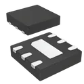
Optical Sensor Ambient I2C 6-UDFN Exposed Pad ## Engineering Specification ## General Description The **MAX44009EDT+T** is an Analog Devices / Maxim Integrated digital ambient light sensor designed for portable electronics, display brightness control, industrial sensors, embedded systems, and low-power optical sensing applications. It integrates an ambient light photodiode, signal conditioning, analog-to-digital conversion, and an I²C digital output interface in a compact surface-mount package. The device is suitable for systems requiring automatic brightness adjustment, low current consumption, and light measurement behavior that closely follows human-eye response. ## Device Identification Manufacturer Part Number: **MAX44009EDT+T** Manufacturer: **Analog Devices / Maxim Integrated** Product Series: **MAX44009** Device Category: **Sensor Integrated Circuit** Device Type: **Digital Ambient Light Sensor** Sensor Interface: **I²C Digital Output** Mounting Type: **Surface Mount** Package Type: **UTDFN-Opto / UDFN** ## Functional Description The device functions as a digital ambient light sensor that measures surrounding light intensity and reports the measurement through an I²C interface. It is designed to help electronic systems adjust display brightness, conserve power, improve user visibility, and respond to changes in lighting conditions. The integrated optical sensing and digital conversion circuitry reduce the need for external analog signal-conditioning components. ## Optical Sensing Description The sensor includes an on-chip photodiode with spectral response optimized to approximate human-eye sensitivity. It also incorporates infrared and ultraviolet blocking capability to improve ambient light measurement accuracy. The adaptive gain function automatically selects the appropriate measurement range, allowing the device to operate across very low-light and bright-light conditions. ## Electrical Description The **MAX44009EDT+T** operates from a low-voltage supply range and is optimized for ultra-low power consumption. It supports digital communication through an I²C interface and is suitable for battery-powered and energy-sensitive systems. Proper supply decoupling, pull-up resistor selection, and bus voltage compatibility should be considered during circuit design. ## Package and Mechanical Description The component is supplied in a compact surface-mount optical package suitable for space-constrained printed circuit board designs. The package is intended for placement where the optical sensing window has access to ambient light while maintaining proper mechanical protection from contamination, shadowing, and enclosure obstruction. ## Interface and Control Description The device communicates with a host microcontroller or processor through an I²C digital interface. The host can read ambient light data and configure device behavior through register-based communication. The selectable I²C addressing feature supports flexible integration in systems that may include multiple I²C peripherals. ## Mounting and Assembly Description The **MAX44009EDT+T** is intended for surface-mount PCB assembly using standard reflow soldering processes. PCB layout should follow the manufacturer’s recommended footprint and assembly guidance. The optical sensing area should remain unobstructed, clean, and aligned with the product enclosure opening or light pipe when used. ## Application Suitability The device is suitable for smartphones, tablets, notebooks, wearable electronics, handheld devices, display brightness control, industrial light sensing, smart home devices, battery-powered equipment, sensor modules, and embedded systems requiring digital ambient light detection. ## Design Considerations The design should account for sensor placement, optical window design, enclosure transparency, light pipe geometry, I²C bus pull-up values, supply voltage compatibility, ambient interference, temperature conditions, and contamination protection. The sensor should not be blocked by opaque materials or placed where shadows, reflections, or nearby LEDs may distort the measured ambient light level. ## Hashtags #commonpartslibrary #integratedcircuit #sensor #ambientlightsensor #digitalsensor #opticalsensor #analogdevices #maximintegrated #max44009 #max44009edt #i2csensor #lightmeasurement #brightnesscontrol #lowpowersensor #portableelectronics #displaycontrol #embeddedhardware #embeddeddesign #smdcomponent #surfacemount #utdfnpackage #uDFNpackage #pcbdesign #hardwaredesign #electronicscomponents #electronicparts #componentlibrary #engineeringparts #electronicsengineering... show more9 Uses
0 Stars
Power Source Selector Module
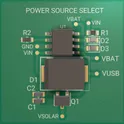
Power Source Selector Module #Module This innovative module is engineered to intelligently manage and select between multiple power sources including battery (VBAT), solar (VSOLAR), USB (VUSB), and VIN. It features a robust design that ensures efficient switching, optimal power regulation, and enhanced diagnostic capabilities. With carefully selected components such as MOSFETs, resistors, LEDs, diodes, and capacitors, this module provides reliable operation across varied load conditions and complex circuit topologies. Its integrated features are perfect for applications requiring seamless transition between renewable energy sources and conventional power, making it an ideal solution for modern, energy-efficient systems. #PCBDesign #Electronics #PowerManagement #Module #CircuitDesign #RenewableEnergy... show more68 Uses
2 Stars
WP483GDT
Green 568nm LED Indication - Discrete 2.2V Radial The WP483GDT is a through-hole green light-emitting diode designed for general-purpose visual indication and low-power lighting applications. It emits a visible green wavelength when forward biased and is commonly used in status indicators, signal displays, and basic illumination circuits. The device is built with a durable epoxy lens package that provides mechanical protection and enhances light output visibility. It is suitable for use in a wide range of electronic systems, including consumer electronics, control panels, and embedded designs. Device Overview The component is a standard discrete LED with a two-lead configuration consisting of an anode and a cathode. It operates by converting electrical energy into light through electroluminescence. The emitted color falls within the green spectrum, making it appropriate for applications requiring clear visual signaling without excessive brightness or power consumption. Electrical Characteristics The LED operates under forward bias conditions, with a typical forward voltage in the range expected for green LEDs. It supports low current operation while maintaining consistent luminous output. Reverse voltage tolerance is limited, and proper polarity must be observed to prevent damage. Current-limiting resistors are required in circuit integration to ensure safe operation. Optical Characteristics The device produces a green light output with a defined luminous intensity and viewing angle based on its lens shape and internal structure. The epoxy lens may be diffused or clear, affecting the spread and focus of the emitted light. Brightness is dependent on the forward current applied. Mechanical Characteristics The LED is housed in a standard round through-hole package, compatible with typical PCB mounting. Leads are spaced to fit common board layouts and can be soldered directly. The epoxy body provides insulation and environmental protection while maintaining optical clarity. Thermal Considerations The device is designed for low power dissipation but should be operated within recommended limits to avoid overheating. Adequate spacing and proper current control help maintain thermal stability and prolong device lifespan. Applications The WP483GDT is suitable for indicator lights in electronic devices, status displays in control systems, educational and hobby electronics, and general-purpose signaling applications where green illumination is required. Compliance and Handling The component should be handled using standard ESD precautions. Storage and soldering conditions should follow typical LED handling practices to maintain performance and reliability. #commonpartslibrary #led #green... show more91 Uses
0 Stars
BP2866C
The BP2866C, manufactured by 晶丰明源半导体, is a high precision buck constant current LED driver designed for universal input offline LED lighting applications. Operating in critical conduction mode, this component is suitable for 85Vac~265Vac input and integrates a 500V power MOSFET. It features patented demagnetization detection technology and high-voltage JFET power supply technology, eliminating the need for a VCC capacitor and starting resistors, thereby minimizing system cost and size. The BP2866C offers precise output current and excellent line regulation through a patent-pending current control method. It includes robust protection functions such as LED short circuit protection, VCC under voltage protection, and thermal regulation. Available in a SOP7 package, it ensures a +5% LED output current accuracy and is ideal for applications like LED candle lights and bulbs.... show more1 Use
0 Stars
TPS543021DRLR
Buck Switching Regulator IC Positive, Isolation Capable Adjustable 0.596V 1 Output 3A SOT-563, SOT-666 The TPS543021DRLR is a compact, integrated power regulator that converts a wide input voltage (typically from batteries or power rails) into a regulated lower output voltage with high efficiency. It includes internal power switches and control circuitry, simplifying power supply design and reducing external component count. Key Features Topology: Synchronous buck converter Input Voltage Range: ~4.5 V to 28 V Output Voltage: Adjustable (via external resistors) Output Current: Up to 3 A continuous Switching Frequency: ~500 kHz (fixed) Efficiency: High efficiency (up to ~90%+) Quiescent Current: Low, suitable for power-sensitive designs Protection Features: Overcurrent protection (OCP) Thermal shutdown Undervoltage lockout (UVLO) Package & Physical Info Package Type: SOT-563 / VSON (compact, no-lead package) Mounting: Surface Mount (SMT) Packaging: Tape & reel (DRLR suffix) #CommonPartsLibrary #IntegratedCircuit #PowerManagement #Voltage-regulator #Switching-regulator... show more33 Uses
0 Stars
LMZ22010TZ/NOPB
Non-Isolated PoL Module DC DC Converter 1 Output 0.8 ~ 6V 10A 6V - 20V Input The LMZ22010TZ/NOPB is a compact, high-efficiency step-down (buck) DC-DC power module from Texas Instruments. It integrates a switching regulator, power MOSFETs, inductor, and compensation components into a single package, simplifying power supply design. This module is capable of delivering up to 10A output current with excellent thermal performance and minimal external components. It is intended for high power density applications such as industrial systems, telecommunications equipment, and embedded processing platforms. Manufacturer Information Manufacturer: Texas Instruments Part Number: LMZ22010TZ/NOPB Product Type: DC-DC Buck Power Module Key Features Integrated power module with inductor and controller Output current up to 10A Wide input voltage range High efficiency operation Adjustable output voltage Built-in protection features (thermal shutdown, overcurrent protection) Power-good output and enable control Requires minimal external components Electrical Characteristics Parameter Value Input Voltage Range 6 V to 20 V Output Voltage Range 0.8 V to 6 V (adjustable) Output Current Up to 10 A Switching Frequency ~500 kHz Efficiency Up to ~95% Operating Temperature Range -40°C to +125°C Package Information Package Type: TO-PMOD (Power Module) Mounting Type: Surface Mount Integrated inductor and power components Optimized for thermal performance Pin Configuration (Typical) Pin Name Description VIN Input supply voltage VOUT Regulated output voltage GND Ground EN Enable input FB Feedback for output adjustment PGOOD Power-good indicator Typical Applications Industrial automation systems Telecom and networking equipment FPGA / DSP / processor power rails Embedded systems Point-of-load regulation Design Considerations Ensure proper PCB layout for heat dissipation Use appropriate input/output capacitors External resistors required to set output voltage Consider airflow for high-current operation #commonpartslibrary #powersupply #dcdc #converter... show more18 Uses
0 Stars
ADPD7000BCBZR7
4 Channel AFE 12 Bit 36-WLCSP (2.8x2.56) The ADPD7000 is a highly integrated analog front end (AFE) designed for measuring various vital signals. The optical channel is designed as an optical transceiver, stimulating up to eight light emitting diodes (LEDs) and measuring the return signal on up to four separate current inputs. The signal chain rejects signal offsets and corruption from asynchronous modulated interference, typically from ambient light, eliminating the need for optical filters or externally controlled DC cancellation circuitry. The electrocardiography (ECG) signal acquisition is designed to support low noise, diagnostic level measurement in the presence of a variety of interferers. The ECG signal chain has a number of complementary features supporting ECG measurement, such as driven reference for common-mode rejection and lead off detection to identify a fallen electrode. The body impedance analysis (BIA) signal chain is designed for body impedance measurement with a configurable excitation path and measurement path. A 12-bit digital-to-analog converter (DAC) is used in the excitation path to generate the sinusoid wave and high precision measurement, with configurable filters used to measure the body response of the stimulus. The electrodermal activity (EDA) signal chain is designed for electrodermal activity. By multiplexing BIA and ECG peripheral circuits, the ADPD7000 supports high precision AC and DC measurement with 1 nS resolution. The data output and functional configuration use a serial port interface (SPI) on the ADPD7000. The control circuitry includes flexible LED signaling and synchronous detection, digital filters, digital wave generators, and configurable filters. The ADPD7000 is available in a 2.795 mm × 2.560 mm, 0.40 mm pitch, 36-ball WLCSP. ► Multimodal analog front end ► Optical channel ► 4 input channels with multiple operation modes for various sensor measurements ► 4-channel processing with simultaneous sampling ► 12 programmable time slots for synchronized sensor measurements ► Flexible input multiplexing to support single-ended sensor measurements ► 8 LED drivers, 2 of which can be driven simultaneously ► Flexible sampling rate from 0.004 Hz to 9 kHz using internal oscillators ► AC ambient light rejection: 78 dB up to 100 Hz ► 400 mA total LED peak drive current ► Individual ambient cancellation DAC at TIA input with 9-bit control up to 300 μA ► Individual LED DC cancellation DAC at TIA input with 7-bit control up to 190 μA ► ECG channel ► <1 µV RMS RTI noise at diagnosis bandwidth ► High input impedance 20 GΩ ► Accepts up to ±1.2 V of DC differential input range ► CMRR: 115 dB ► Flexible 4 electrode configurations to support various applications ► Both AC lead off detection and DC lead off detection ► Support always on, low power, lead on detection ► BIA channel ► Low power, high accuracy excitation path ► Configurable excitation frequency up to 250 kHz ► Sine wave excitation with a 12-bit DAC ► High accuracy with large imbalance contact impedance ≤20 kΩ ► Configurable receive filters with low noise design ► Complex impedance measurement engine ► Integrated current-limit resistors ► EDA channel ► Support both voltage excitation and current excitation ► 10 kΩ to100 MΩ measurement range with 1 nS resolution ► DFT and decimation for high accuracy measurement result ► SPI communications supported ► 704-byte FIFO... show more4 Uses
0 Stars
MAX1555 Module
This project is a battery charging circuit utilizing a MAX1555 chip. It features a USB and DC power input, with LED status indicators. The design is outfitted with necessary decoupling capacitors and resistors to ensure smooth operation. #project #Template #charger #reusable #module #batterycharger #MAX1555 #template #bms #analog... show more0 Uses
0 Stars