Attachment Review

see the mechanical specification and pin config
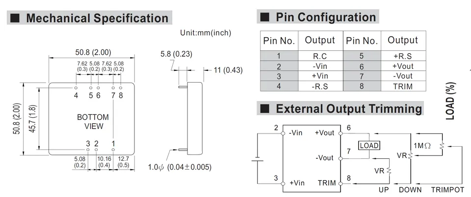
Image
Thought for 10 sec
Yes — I see it: the SKA60 uses a non-uniform 8-pin bottom-view pattern, not a simple 5.08mm grid. I’ll check the current U1 footprint against those coordinates and record/fix the footprint risk.
Worked for 5 mins 40 sec
Updated U1 to match the attached SKA60 mechanical spec: the footprint now uses the non-uniform bottom-view 8-pin pattern and 1.3mm drilled / 2.2mm pads for the 1.0mm pins.
Open items:
- The published custom part may still need the same footprint correction; I applied overrides in this project layout.
- DRC still reports airwires because routing has not been done yet.
Documented here: PCB Layout Notes.
Fix part, route, review
Fix custom part
Route the board
Run full DRC
Explain pin pattern
Refine this doc
Ask about this doc
Schematic Design Notes
Current Schematic Status
- Main schematic capture is complete for the requested power-distribution architecture.
- Electrical checks currently show no open schematic ERC warnings/errors for floating pins, no-connects, pin-to-pin conflicts, power pins, single-pin nets, or undriven nets.
- PCB DRC airwire/overlap errors are expected at this stage because no PCB placement/routing has been performed yet.
Implemented Blocks
- J1: 24V DC input, Phoenix Contact 1803277 / MC 1,5/ 2-G-3,81, 3.81mm pitch, right-angle pluggable header.
- F1: 5x20mm PCB fuse holder for a 4A slow-blow cartridge fuse.
- F2: RUEF200 30V-class 2A-hold PTC for the 24V pass-through output branch.
- J2: protected 24V output terminal block.
- U1: Mean Well SKA60B-12 24V input to 12V/5A isolated DC-DC module.
- F3/F4: Littelfuse 16R160B radial PTCs for 12V OUT 1 and OUT 2.
- F5: Littelfuse 16R185B radial PTC for 12V OUT 3.
- J3/J4/J5: protected 12V output terminal blocks.
- C1: 1uF/50V ceramic across 24V input near U1.
- C2: 100uF/25V electrolytic across the 12V rail near U1.
- C3: 1uF/25V ceramic across the 12V rail near U1.
- D1/R1: 24V green indicator LED with 2.2kΩ, 0.5W resistor.
- D2/R2: 12V green indicator LED with 1kΩ resistor.
- MH1-MH4: 3.2mm non-copper NPTH mounting holes for M3 screws.
Net Assignments
Table
| Net | Function | Current Class |
|---|---|---|
| 24V_IN_RAW | J1 positive input before fuse | 5A board-copper target |
| 24V_FUSED | Fused 24V bus after F1 feeding U1, F2, C1, and D1/R1 | 4A fuse-limited nominal |
| 24V_OUT | F2-protected 24V output to J2 | 2A branch |
| 12V | U1 output rail feeding C2/C3, D2/R2, and F3/F4/F5 | 5A max |
| 12V_OUT1 | F3-protected 12V output to J3 | 1.6A nominal PTC hold |
| 12V_OUT2 | F4-protected 12V output to J4 | 1.6A nominal PTC hold |
| 12V_OUT3 | F5-protected 12V output to J5 | 1.85A nominal PTC hold |
| GND | Common negative; input and output negatives intentionally tied | 5A return target |
Datasheet-Backed Custom Parts Created
- SKA60B-12: /beedo/ska60b-12
- 16R160B: /beedo/16r160b
- 16R185B: /beedo/16r185b
- RUEF200: /beedo/ruef200
Engineering Notes and Risks
- A 16V PTC is not suitable on the 24V pass-through branch, so the 24V branch uses a 30V-class RUEF200 instead.
- The 16R160B and 16R185B 12V branch PTCs have room-temperature hold-current ratings. Their hold current must be derated for 60°C enclosed ambient.
- The third 12V branch uses 16R185B because the exact Littelfuse USBR 2.0A radial 16V value was not available in the sourced USBR table. If true 2.0A continuous hold at 60°C is required, the part should be revisited.
- The 4A slow-blow input fuse may be marginal if the SKA60B-12 is near 60W output and the 24V pass-through branch is loaded simultaneously, especially near the module's 18V minimum input where converter input current rises.
- The SKA60B-12 output capacitance is 100uF + 1uF locally, below the stated 220uF external capacitance limit. Downstream load capacitance should also be considered.
- No reverse-polarity protection or TVS/transient clamp has been added yet; field wiring and long 24V leads may justify adding these before layout release.
- Common negative is intentional and defeats downstream isolation benefits of the SKA60B-12.
- Layout must use pours/wide copper, avoid narrow neck-downs around connectors/fuse/PTCs, and keep PTCs thermally separated from U1.
- Current DRC airwire/overlap findings are expected until placement and routing are performed.
Current Schematic Status
Implemented Blocks
Net Assignments
Datasheet-Backed Custom Parts Created
Engineering Notes and Risks
