Attachment Review

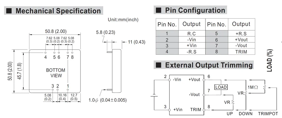
see the mechanical specification and pin config
Image
Thought for 10 sec
Yes — I see it: the SKA60 uses a non-uniform 8-pin bottom-view pattern, not a simple 5.08mm grid. I’ll check the current U1 footprint against those coordinates and record/fix the footprint risk.
Worked for 5 mins 40 sec
Updated U1 to match the attached SKA60 mechanical spec: the footprint now uses the non-uniform bottom-view 8-pin pattern and 1.3mm drilled / 2.2mm pads for the 1.0mm pins.
Open items:
- The published custom part may still need the same footprint correction; I applied overrides in this project layout.
- DRC still reports airwires because routing has not been done yet.
Documented here: PCB Layout Notes.
Fix part, route, review
Fix custom part
Route the board
Run full DRC
Explain pin pattern
Refine this doc
Ask about this doc
PCB Layout Notes
Board Setup
- Board outline set to 75mm × 75mm rectangle with 2mm corner radius.
- Stackup set to Standard 2 Layer.
- Universal keepout / board inset set to 1mm.
- 75mm width is treated as the hard maximum. Depth was set to the allowed 75mm maximum because the SKA60B-12 module and connector/protection hardware make the board extremely dense.
Added Input Protection
- Q1: QM6015D P-channel MOSFET added as high-side reverse-polarity protection.
- F1 output / TVS / Q1 drain net: 24V_FUSED_PRE_REV.
- Q1 source / protected load side: 24V_FUSED.
- Q1 gate net: Q1_GATE.
- D3: SMBJ33A TVS from 24V_FUSED_PRE_REV to GND.
- D4: BZX79C12 12V zener clamp from Q1 source to Q1 gate.
- R3: 100kΩ gate pull-down from Q1_GATE to GND.
Placement Summary
- J1-J5 are placed in a straight row along the bottom long edge, ordered J1, J2, J3, J4, J5.
- U1 SKA60B-12 is centered above the connector row.
- F1 and input protection parts are grouped near J1.
- F2-F5 are near their corresponding output connectors.
- MH1-MH4 are placed at the four board corners.
- D1/D2 indicators are placed near the right/visible edge.
- To fit inside the 75mm × 75mm limit, small support parts C1, C2, C3, R3, D3, and D4 are on the bottom layer. Major connectors, fuse/PTCs, SKA60 module, LEDs, and mounting holes remain on the top layer.
SKA60B-12 Mechanical Pin Pattern
The attached Mean Well SKA60 datasheet shows a non-uniform 8-pin bottom-view footprint, not a simple 5.08mm grid. U1 pad overrides were applied in the PCB layout using the datasheet mechanical drawing.
Using the 50.8mm × 50.8mm body center as the footprint origin, the U1 pad positions are:
Table
| Pin | Function | X from body center | Y from body center |
|---|---|---|---|
| 1 | R.C | 20.32mm | 10.16mm |
| 2 | -Vin | 12.70mm | 10.16mm |
| 3 | +Vin | 5.08mm | 10.16mm |
| 4 | -R.S | 5.08mm | -2.54mm |
| 5 | +R.S | 12.70mm | -2.54mm |
| 6 | +Vout | 20.32mm | -2.54mm |
| 7 | -Vout | 12.70mm | 20.32mm |
| 8 | TRIM | 20.32mm | 20.32mm |
All U1 pads were set as through-hole pads with 1.3mm drills and 2.2mm circular pads for the datasheet's 1.0mm diameter pins. These are project-level footprint overrides; verify against the physical module before fabrication.
DRC / Review Status After Placement
- No component-overlap or out-of-board placement errors are currently reported.
- Airwires remain because routing has not been performed yet. This is expected after placement.
- Manufacturing review still flags missing MPNs for generic passives and the generic fuse holder:
- C1, C2, C3
- R1, R2, R3
- F1
- Board density remains critical at approximately 77.6% component-area fill. The layout is possible only by using the bottom layer for small support passives; single-sided assembly inside 75mm × 75mm is not realistic with the current component set.
Layout Risks / Next Actions
- Routing should use wide copper pours for 24V_FUSED, 24V_OUT, 12V, and GND rather than narrow traces.
- Bottom GND pour should be preserved for return current, but bottom passives now occupy some of that layer.
- PTCs are near the connector row and close to U1 due to space limits; thermal validation at 60°C enclosed ambient remains required.
- Before manufacturing, assign exact MPNs for generic passives and F1, then route power first and rerun DRC.
Board Setup
Added Input Protection
Placement Summary
SKA60B-12 Mechanical Pin Pattern
DRC / Review Status After Placement
Layout Risks / Next Actions
