Attachment Review

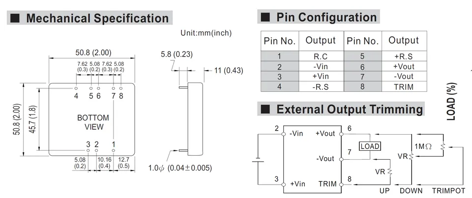
see the mechanical specification and pin config
Image
Thought for 10 sec
Yes — I see it: the SKA60 uses a non-uniform 8-pin bottom-view pattern, not a simple 5.08mm grid. I’ll check the current U1 footprint against those coordinates and record/fix the footprint risk.
Worked for 5 mins 40 sec
Updated U1 to match the attached SKA60 mechanical spec: the footprint now uses the non-uniform bottom-view 8-pin pattern and 1.3mm drilled / 2.2mm pads for the 1.0mm pins.
Open items:
- The published custom part may still need the same footprint correction; I applied overrides in this project layout.
- DRC still reports airwires because routing has not been done yet.
Documented here: PCB Layout Notes.
Fix part, route, review
Fix custom part
Route the board
Run full DRC
Explain pin pattern
Refine this doc
Ask about this doc
Project Specification
Project Overview
Status: Draft
Design a low-voltage DC power distribution PCB mounted behind a standard Australian faceplate. The board accepts 24V DC input, provides a fused 24V pass-through output, and generates a 12V/5A rail via a Mean Well SKA60B-12 isolated DC-DC module for three individually protected 12V outputs.
Intended Use
- Enclosed recessed wall box installation, convection cooling only.
- Continuous unattended operation.
- Internal ambient up to 60°C.
- Prototype / production-intent hobbyist build; prioritize mechanical robustness and serviceability.
What the Device Should Do
- Accept nominal 24V DC input.
- Fuse the incoming +24V before the 24V output and DC-DC module input.
- Provide one protected 24V pass-through output for a PoE injector feed.
- Convert 24V to 12V at up to 5A using the SKA60B-12 module.
- Split the 12V rail into three protected outputs.
- Show 24V and 12V rail presence with green 3mm LEDs.
Main Features
- 2-layer PCB, single-sided assembly.
- Maximum board envelope: 75 × 75 mm.
- Connector row along one long edge.
- Through-hole preferred for all power components.
- Phoenix Contact MC-series 3.81 mm pluggable terminal blocks acceptable/preferred to recover board-edge space.
- Four M3 mounting holes at corners.
System Architecture
Diagram
Hardware Subsystems
Input and 24V Distribution
- J1: 2-pin 24V DC input, Phoenix MC 3.81 mm right-angle pluggable header target.
- F1: 5 × 20 mm PCB fuse holder with 4A slow-blow fuse in series with +24V input.
- J2: 2-pin fused 24V DC output with 2A-hold PTC protection requested for pass-through output.
- 1uF ceramic capacitor across 24V input near DC-DC module.
- 24V green LED with 2.2kΩ series resistor.
12V Conversion and Distribution
- U1: Mean Well SKA60B-12, 2 × 2 inch / 50.8 × 50.8 mm, 8-pin through-hole module.
- Pin requirements from user-supplied spec:
- Pin 1 R.C: leave unconnected.
- Pin 2 -Vin: connect to common negative.
- Pin 3 +Vin: connect to fused +24V.
- Pin 4 -R.S: tie directly to -Vout at module pins.
- Pin 5 +R.S: tie directly to +Vout at module pins.
- Pin 6 +Vout: +12V output rail.
- Pin 7 -Vout: common negative.
- Pin 8 TRIM: leave unconnected.
- 100uF/25V electrolytic + 1uF ceramic across 12V rail near module output. Total external capacitance must remain under SKA60 220uF limit.
- Three 12V outputs with resettable PTCs: two 1.5A hold, one 2A hold, minimum 16V rated.
- 12V green LED with 1kΩ series resistor.
Interfaces and Connections
- J1: 24V IN, polarity labelled.
- J2: 24V OUT, polarity labelled, PoE injector feed.
- J3: 12V OUT 1, polarity labelled.
- J4: 12V OUT 2, polarity labelled.
- J5: 12V OUT 3, polarity labelled.
- All five connectors on the same board edge, right-angle entry, plug supplied with loom.
Power and Runtime Expectations
- 24V input path and 24V output: design target 5A continuous copper capacity.
- 12V rail: 5A continuous maximum from DC-DC module.
- Individual 12V outputs: up to protected branch current, max 2A branch.
- Continuous unattended operation in warm enclosure.
Power Tree and Power Budget
Table
| Path | Nominal Voltage | Protection | Continuous Design Target |
|---|---|---|---|
| Input before fuse | 24V | External source protection TBD | 5A board copper target |
| Fused 24V bus | 24V | 4A slow-blow fuse | 4A fuse-limited total unless changed |
| 24V output branch | 24V | 2A-hold PTC | 2A branch hold target |
| DC-DC input | 24V | Behind 4A fuse | Sized by SKA60 input current |
| 12V rail | 12V | SKA60 module current limit | 5A max |
| 12V OUT 1 | 12V | 1.5A-hold PTC | 1.5A hold |
| 12V OUT 2 | 12V | 1.5A-hold PTC | 1.5A hold |
| 12V OUT 3 | 12V | 2A-hold PTC | 2A hold |
Important sizing note: 12V at 5A is 60W. At 24V input, converter input current is roughly 2.5A at 100% efficiency and higher in practice. If the 24V pass-through output can also draw 2A, the upstream 4A fuse may nuisance-trip or limit combined full-load operation depending on module efficiency and ambient derating. This needs verification against the SKA60B-12 datasheet and final load assumptions.
Manufacturing and Assembly Expectations
- 2-layer PCB.
- 1oz copper minimum; 2oz preferred.
- Power traces implemented as copper pours or at least 3mm trace width.
- Bottom layer common negative pour.
- Single-sided assembly preferred.
- Through-hole power components preferred.
- No components taller than SKA60 module height of 11mm except fuse holder and connectors.
Firmware-Relevant Hardware Requirements
No firmware or microcontroller required.
Physical Design Expectations
- Maximum PCB envelope: 75 × 75 mm.
- Must fit behind standard Australian faceplate/aperture zone with clearance.
- Connector row along one long edge.
- Polyfuses spaced away from SKA60 module body for thermal derating.
- LED positions should be visible through or near the faceplate if possible.
- Four M3 mounting holes at corners.
Important Design Decisions
- Use SKA60B-12 module now that 75 × 75 mm envelope is allowed.
- Use Phoenix MC 3.81 mm pluggable connectors instead of 5.08 mm MSTB to reduce connector-row width.
- Common negative allowed; module isolation does not need to be maintained downstream.
- R.C and TRIM left unconnected; remote sense pins tied locally at module output pins.
Assumptions
- Nominal input is 24V DC from a suitably current-limited SELV/LVDC supply.
- Phoenix MC-series current rating selected will be verified against exact MPN and derating.
- Final fuse/connector/PTC MPNs will be selected from available library parts or datasheet-backed alternatives.
- Exact faceplate/window/mechanical keepout drawing is not yet provided; 75 × 75 mm is treated as the allowed PCB envelope for now.
Change Notes
- Width/height constraint corrected from 70 × 45 mm to up to 75 × 75 mm.
- Connector pitch direction changed to Phoenix MC-series 3.81 mm to recover approximately 12–15 mm along the connector edge.
Project Overview
Intended Use
What the Device Should Do
Main Features
System Architecture
Hardware Subsystems
Input and 24V Distribution
12V Conversion and Distribution
Interfaces and Connections
Power and Runtime Expectations
Power Tree and Power Budget
Manufacturing and Assembly Expectations
Firmware-Relevant Hardware Requirements
Physical Design Expectations
Important Design Decisions
Assumptions
Change Notes
