Part Data Review and Validation
0:58
Evalu.
Analyzing the schematic.
Reviewing the bill of materials.
Analyzing the PCB layout.
Looking for "part description, ordering information, package type, package designation, and pin count" in datasheet
Looking for "special features and product highlights" in datasheet
Looking for "absolute maximum ratings" in datasheet
Looking for "recommended operating conditions" in datasheet
Looking for "electrical characteristics" in datasheet
Looking for "pin configuration and function descriptions" in datasheet
Looking for "package information mechanical dimensions for the BCPZ package" in datasheet
Assess.
Review.
- The part already has a datasheet URL set in project properties: Datasheet
- Because a datasheet URL was already present, there was no need to search the web or update properties.
Project metadata
| Field | Value |
|---|---|
| Description | Single-Ended Input, Quad, Simultaneous Sampling, 16-Bit/14-Bit/12-Bit, SAR ADC |
| Manufacturer | Analog Devices |
| MPN | AD7386-4BCPZ |
| Datasheet | Datasheet |
Datasheet package / ordering metadata
| Field | Value |
|---|---|
| Family | AD7386-4 / AD7387-4 / AD7388-4 |
| Orderable part | AD7386-4BCPZ |
| Other order codes | AD7386-4BCPZ-RL, AD7386-4BCPZ-RL7 |
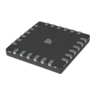
| Package | 24-lead LFCSP |
| Package designation | CP-24-25 |
| Body size | 4 mm x 4 mm |
| Package height | 0.55 mm nominal, 0.60 mm max |
| Lead pitch | 0.50 mm BSC |
| Exposed pad | Present, must be connected to GND |
Special features
| Feature | Value |
|---|---|
| ADC type | Quad simultaneous-sampling SAR ADC |
| Input type | Single-ended analog inputs |
| Resolution family | 16-bit / 14-bit / 12-bit |
| Max throughput | 4 MSPS |
| Oversampling | On-chip oversampling, 2-bit resolution boost |
| Alert | Out-of-range indicator |
| Reference | 2.5 V internal reference available |
| Logic interface supply | Separate logic supply supports 1.65 V to 3.6 V |
| Temperature range | -40 C to +125 C |
Recommended operating conditions
| Parameter | Value |
|---|---|
| VCC | 3.0 V to 3.6 V |
| VLOGIC | 1.65 V to 3.6 V |
| External VREF at REFIO | 2.5 V to 3.3 V |
| Sample rate | Up to 4 MSPS |
| Ambient temperature | -40 C to +125 C |
Absolute maximum ratings
| Parameter | Rating |
|---|---|
| VCC to GND | -0.3 V to +4 V |
| VLOGIC to GND | -0.3 V to +4 V |
| Analog input to GND | -0.3 V to VREF + 0.3 V, or VCC + 0.3 V |
| Digital input to GND | -0.3 V to VLOGIC + 0.3 V |
| Digital output to GND | -0.3 V to VLOGIC + 0.3 V |
| REFIO to GND | -0.3 V to VCC + 0.3 V |
| Input current except supplies | +-10 mA |
| Operating temperature | -40 C to +125 C |
| Storage temperature | -65 C to +150 C |
| Max junction temperature | 150 C |
| Pb-free reflow | 260 C |
Key electrical characteristics from the datasheet
| Parameter | Value |
|---|---|
| Resolution | 16 bits |
| Conversion rate, single-channel pair | 4 MSPS typ |
| Conversion rate, alternating channels | 2 MSPS typ |
| No missing codes | 16 bits |
| DNL | -0.99 / +-0.6 / +1.0 LSB |
| INL, external reference | -7 / +-4 / +7 LSB |
| INL, internal reference | +-3 LSB typ |
| Gain error, external reference 3.3 V | -0.08 / +-0.005 / +0.08 % FS |
| Offset error, external reference | -1 / +-0.07 / +0.1 mV |
| Dynamic range, VREF = 3.3 V | 86 dB typ |
| SNR, VREF = 3.3 V | 84.7 dB typ |
| SNR, VREF = 2.5 V internal | 81.7 dB typ |
| SNR with OSR = 8 | 92 dB typ |
| SFDR | -103 dB typ |
| THD | -100 dB typ |
| SINAD, VREF = 3.3 V | 84.5 dB typ |
| IVCC normal mode | 45 mA typ |
| Total power dissipation | 191 mW typ |
Datasheet pin map
| Pin | Name | Datasheet function |
|---|---|---|
| 1, 5, 14, 16 | GND | Ground reference points |
| 2 | VLOGIC | Logic supply, decouple to GND with 1 uF |
| 3 | REGCAP | Internal regulator decoupling, 1 uF to GND, 1.9 V typ |
| 4 | VCC | Main supply, decouple to GND with 1 uF |
| 6, 7 | AIND1, AIND0 | ADC D analog inputs |
| 8, 9 | AINC1, AINC0 | ADC C analog inputs |
| 10, 11 | AINB1, AINB0 | ADC B analog inputs |
| 12, 13 | AINA1, AINA0 | ADC A analog inputs |
| 15 | REFCAP | Band-gap reference decoupling, 0.1 uF to GND, 2.5 V typ |
| 17 | REFIO | Reference input/output, 2.5 V to 3.3 V external reference allowed, 1 uF decoupling required |
| 18 | CS | Active-low chip select |
| 19 | SDOA | Serial data output A |
| 20 | SDOB | Serial data output B |
| 21 | SDI | Serial data input |
| 22 | SCLK | Serial clock input |
| 23 | SDOC | Serial data output C |
| 24 | SDOD/ALERT | Serial data output D or alert output |
| EPAD | Exposed pad | Must be connected to GND |
Mechanical data
| Parameter | Value |
|---|---|
| Package code | CP-24-25 |
| Package style | 24-Lead LFCSP |
| Body | 4.10 / 4.00 / 3.90 mm square |
| Height | 0.60 / 0.55 / 0.50 mm |
| Lead pitch | 0.50 mm BSC |
| Terminal width | 0.30 / 0.25 / 0.20 mm |
| Exposed pad size | 0.60 / 0.50 / 0.40 mm square |
| Coplanarity | 0.08 mm |
What matches
| Check | Result | Notes |
|---|---|---|
| MPN | Pass | Project MPN matches datasheet orderable part |
| Package family | Pass | Footprint is a 4 mm x 4 mm, 0.50 mm pitch 24-lead QFN/LFCSP style with center pad |
| Lead count | Pass | Datasheet says 24 leads plus exposed pad; project footprint has 25 pads total |
| Pin numbering | Pass | Symbol pin numbers 1-25 align with footprint pad numbering 1-25 |
| Signal naming | Pass | Signal names align with datasheet names |
| Center pad presence | Pass | Footprint includes pad 25 for the exposed pad |
Issues and risks
| Severity | Finding | Why it matters |
|---|---|---|
| Medium | The exposed pad is represented as pin 25 named GND_5 instead of EPAD | Electrically this is likely fine if tied to ground, but it is semantically different from the datasheet and can confuse users, reviews, and reuse of the part |
| Medium | All symbol pins are typed as Unspecified | This will not break fabrication directly, but it weakens ERC and can hide connection mistakes in downstream designs |
| Low | Footprint asset name is generic QFN-style (QFN50P400X400X60-25N-D) while datasheet package is LFCSP CP-24-25 | Geometry appears consistent, so this is not an immediate failure risk, but package naming mismatch can cause ordering/review confusion if someone assumes strict package naming |
| Low | I could not verify paste-mask segmentation, courtyard policy, or assembly land pattern intent beyond the raw footprint definition returned | These details can affect assembly yield on small exposed-pad packages, though no obvious fatal mismatch was visible |
- No obvious fatal symbol-to-footprint mismatch was found.
- The part appears largely consistent with the datasheet for:
- AD7386-4BCPZ
- 24-lead 4 mm x 4 mm LFCSP
- 0.50 mm pitch
- exposed pad present
- The main cleanup item is to rename/document pin 25 as the exposed pad function and assign proper pin electrical types.
Highest-priority corrections
| Priority | Recommended correction |
|---|---|
| 1 | Rename or document pad/pin 25 explicitly as EPAD/GND |
| 2 | Set correct pin types for supplies, grounds, inputs, outputs, and digital pins |
| 3 | Optionally align package naming in properties with CP-24-25, 24-lead LFCSP to reduce ambiguity |
Ready.
Reviews

- Wirelessly connects nets on schematic. Used to organize schematics and separate functional blocks. To wirelessly connect net portals, give them same designator. #portaljharwinbarrozo43.0M
- Wirelessly connects power nets on schematic. Identical to the net portal, but with a power symbol. Used to organize schematics and separate functional blocks. To wirelessly connect power net portals, give them the same designator. #portal #powerjharwinbarrozo11.4M
- A generic fixed resistor ideal for rapid circuit topology development. Its footprint automatically adapts based on the selected package case code—supporting 0402, 0603, 0805, 1203, and many other standard SMD packages, as well as axial horizontal and vertical configurations. Save precious design time by seamlessly add more information to this part (value, footprint, etc.) as it becomes available. Standard resistor values: 1.0 ohm, 10 ohm, 100 ohm, 1.0k ohm, 10k ohm, 100k ohm, 1.0M ohm 1.1 ohm, 11 ohm, 110 ohm, 1.1k ohm, 11k ohm, 110k ohm, 1.1M ohm 1.2 ohm, 12 ohm, 120 ohm, 1.2k ohm, 12k ohm, 120k ohm, 1.2M ohm 1.3 ohm, 13 ohm, 130 ohm, 1.3k ohm, 13k ohm, 130k ohm, 1.3M ohm 1.5 ohm, 15 ohm, 150 ohm, 1.5k ohm, 15k ohm, 150k ohm, 1.5M ohm 1.6 ohm, 16 ohm, 160 ohm, 1.6k ohm, 16k ohm, 160k ohm, 1.6M ohm 1.8 ohm, 18 ohm, 180 ohm, 1.8K ohm, 18k ohm, 180k ohm, 1.8M ohm 2.0 ohm, 20 ohm, 200 ohm, 2.0k ohm, 20k ohm, 200k ohm, 2.0M ohm 2.2 ohm, 22 ohm, 220 ohm, 2.2k ohm, 22k ohm, 220k ohm, 2.2M ohm 2.4 ohm, 24 ohm, 240 ohm, 2.4k ohm, 24k ohm, 240k ohm, 2.4M ohm 2.7 ohm, 27 ohm, 270 ohm, 2.7k ohm, 27k ohm, 270k ohm, 2.7M ohm 3.0 ohm, 30 ohm, 300 ohm, 3.0K ohm, 30K ohm, 300K ohm, 3.0M ohm 3.3 ohm, 33 ohm, 330 ohm, 3.3k ohm, 33k ohm, 330k ohm, 3.3M ohm 3.6 ohm, 36 ohm, 360 ohm, 3.6k ohm, 36k ohm, 360k ohm, 3.6M ohm 3.9 ohm, 39 ohm, 390 ohm, 3.9k ohm, 39k ohm, 390k ohm, 3.9M ohm 4.3 ohm, 43 ohm, 430 ohm, 4.3k ohm, 43K ohm, 430K ohm, 4.3M ohm 4.7 ohm, 47 ohm, 470 ohm, 4.7k ohm, 47k ohm, 470k ohm, 4.7M ohm 5.1 ohm, 51 ohm, 510 ohm, 5.1k ohm, 51k ohm, 510k ohm, 5.1M ohm 5.6 ohm, 56 ohm, 560 ohm, 5.6k ohm, 56k ohm, 560k ohm, 5.6M ohm 6.2 ohm, 62 ohm, 620 ohm, 6.2k ohm, 62K ohm, 620K ohm, 6.2M ohm 6.8 ohm, 68 ohm, 680 ohm, 6.8k ohm, 68k ohm, 680k ohm, 6.8M ohm 7.5 ohm, 75 ohm, 750 ohm, 7.5k ohm, 75k ohm, 750k ohm, 7.5M ohm 8.2 ohm, 82 ohm, 820 ohm, 8.2k ohm, 82k ohm, 820k ohm, 8.2M ohm 9.1 ohm, 91 ohm, 910 ohm, 9.1k ohm, 91k ohm, 910k ohm, 9.1M ohm #generics #CommonPartsLibraryjharwinbarrozo1.5M
- A generic fixed capacitor ideal for rapid circuit topology development. You can choose between polarized and non-polarized types, its symbol and the footprint will automatically adapt based on your selection. Supported options include standard SMD sizes for ceramic capacitors (e.g., 0402, 0603, 0805), SMD sizes for aluminum electrolytic capacitors, and through-hole footprints for polarized capacitors. Save precious design time by seamlessly add more information to this part (value, footprint, etc.) as it becomes available. Standard capacitor values: 1.0pF, 10pF, 100pF, 1000pF, 0.01uF, 0.1uF, 1.0uF, 10uF, 100uF, 1000uF, 10000uF 1.1pF, 11pF, 110pF, 1100pF 1.2pF, 12pF, 120pF, 1200pF 1.3pF, 13pF, 130pF, 1300pF 1.5pF, 15pF, 150pF, 1500pF, 0.015uF, 0.15uF, 1.5uF, 15uF, 150uF, 1500uF 1.6pF, 16pF, 160pF, 1600pF 1.8pF, 18pF, 180pF, 1800pF 2.0pF, 20pF, 200pF, 2000pF 2.2pF, 22pF, 220pF, 2200pF, 0.022uF, 0.22uF, 2.2uF, 22uF, 220uF, 2200uF 2.4pF, 24pF, 240pF, 2400pF 2.7pF, 27pF, 270pF, 2700pF 3.0pF, 30pF, 300pF, 3000pF 3.3pF, 33pF, 330pF, 3300pF, 0.033uF, 0.33uF, 3.3uF, 33uF, 330uF, 3300uF 3.6pF, 36pF, 360pF, 3600pF 3.9pF, 39pF, 390pF, 3900pF 4.3pF, 43pF, 430pF, 4300pF 4.7pF, 47pF, 470pF, 4700pF, 0.047uF, 0.47uF, 4.7uF, 47uF, 470uF, 4700uF 5.1pF, 51pF, 510pF, 5100pF 5.6pF, 56pF, 560pF, 5600pF 6.2pF, 62pF, 620pF, 6200pF 6.8pF, 68pF, 680pF, 6800pF, 0.068uF, 0.68uF, 6.8uF, 68uF, 680uF, 6800uF 7.5pF, 75pF, 750pF, 7500pF 8.2pF, 82pF, 820pF, 8200pF 9.1pF, 91pF, 910pF, 9100pF #generics #CommonPartsLibraryjharwinbarrozo1.5M
- A generic fixed inductor suitable for rapid circuit topology development. The footprint automatically adapts based on the selected package, supporting standard SMD sizes (e.g., 0402, 0603, 0805) as well as well-known inductor packages such as SDR1806, PA4320, SRN6028, and SRR1260. Standard inductor values: 1.0 nH, 10 nH, 100 nH, 1.0 µH, 10 µH, 100 µH, 1.0 mH 1.2 nH, 12 nH, 120 nH, 1.2 µH, 12 µH, 120 µH, 1.2 mH 1.5 nH, 15 nH, 150 nH, 1.5 µH, 15 µH, 150 µH, 1.5 mH 1.8 nH, 18 nH, 180 nH, 1.8 µH, 18 µH, 180 µH, 1.8 mH 2.2 nH, 22 nH, 220 nH, 2.2 µH, 22 µH, 220 µH, 2.2 mH 2.7 nH, 27 nH, 270 nH, 2.7 µH, 27 µH, 270 µH, 2.7 mH 3.3 nH, 33 nH, 330 nH, 3.3 µH, 33 µH, 330 µH, 3.3 mH 3.9 nH, 39 nH, 390 nH, 3.9 µH, 39 µH, 390 µH, 3.9 mH 4.7 nH, 47 nH, 470 nH, 4.7 µH, 47 µH, 470 µH, 4.7 mH 5.6 nH, 56 nH, 560 nH, 5.6 µH, 56 µH, 560 µH, 5.6 mH 6.8 nH, 68 nH, 680 nH, 6.8 µH, 68 µH, 680 µH, 6.8 mH 8.2 nH, 82 nH, 820 nH, 8.2 µH, 82 µH, 820 µH, 8.2 mH #generics #CommonPartsLibraryjharwinbarrozo15.7k
- An electrical connector acting as reusable interface to a conductor and creating a point where external circuits can be connected.Terminal
- 47 kOhms ±5% 0.125W, 1/8W Chip Resistor 0805 (2012 Metric) Automotive AEC-Q200 Thick Film #forLedBlinkjharwinbarrozo1.2M
- 10uF Capacitor Aluminum Polymer 20% 16V SMD 5x5.3mm #forLedBlink #commonpartslibrary #capacitor #aluminumpolymer #radialcanjharwinbarrozo1.2M
- Yellow 595nm LED Indication - Discrete 1.7V 1206 (3216 Metric) #forLedBlinkjharwinbarrozo1.1M


AD7386-4BCPZ
Properties
AD7386-4BCPZ
Analog Devices
Integrated Circuit
IC
Pricing & Availability
See prices from popular manufacturers for your project.
Controls
Welcome 👋
Flux accelerates your PCB design with AI.
Create your account to start using this component and bring your ideas to life.