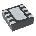
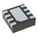
IHDM1008BCEV4R7M30
4.7 µH Unshielded Drum Core, Wirewound Inductor 62 A 0.95mOhm Max Vertical, 2 PC Pin The IHDM1008BCEV4R7M30 is a surface-mount power inductor designed for energy storage and filtering in switching power supplies and DC-DC converter circuits. It provides stable inductance characteristics under varying current conditions, making it suitable for applications requiring efficient power conversion and noise suppression. The device is constructed using a magnetically shielded structure to minimize electromagnetic interference and ensure reliable operation in densely populated circuit environments. Its design supports high current handling capability while maintaining low core losses, contributing to overall system efficiency. Functional Overview The inductor stores energy in its magnetic field when current flows through it and releases that energy when the current changes. This behavior is essential for smoothing current in switching regulators and maintaining stable voltage levels in power circuits. Its low resistance winding helps reduce power loss, while the magnetic shielding limits flux leakage, improving performance in sensitive electronic systems. The component is optimized for high-frequency operation typically found in modern power management designs. Electrical Characteristics The device provides a fixed inductance value with stable performance across a range of operating currents. It supports relatively high saturation current levels, allowing it to function effectively in power circuits without significant degradation of inductance. Low direct current resistance contributes to improved efficiency and reduced heat generation. The inductor is designed to maintain consistent electrical behavior across typical operating temperatures and frequencies used in switching applications. Interface Requirements The component features standard surface-mount terminals for direct placement onto printed circuit boards. Proper soldering and pad design are required to ensure mechanical stability and optimal electrical performance. Placement considerations should include minimizing loop area and proximity to switching elements to reduce noise and maximize efficiency. Operating Conditions The inductor is intended for operation across a wide temperature range suitable for consumer and industrial electronics. It is capable of maintaining performance under continuous load conditions and varying thermal environments. Adequate thermal management and airflow may be necessary in high-current applications to prevent excessive temperature rise. Protection and Reliability Features The device is constructed with durable materials to ensure long-term reliability under electrical and thermal stress. Its magnetically shielded design reduces susceptibility to external interference and limits emissions that could affect nearby components. It is designed to withstand standard handling and soldering processes associated with surface-mount assembly. Packaging and Integration The IHDM1008BCEV4R7M30 is provided in a compact surface-mount package optimized for automated assembly processes. Its form factor allows efficient use of board space while supporting high-performance power designs. The package design ensures secure mounting and consistent electrical contact in high-density circuit layouts. Applications Typical applications include DC-DC converters, voltage regulator modules, power management circuits, filtering stages, and energy storage elements in portable devices, industrial equipment, and communication systems. #commonpartslibrary #inductors... show more0 Uses
0 Stars
WS72324Q-16/TR
WS72324Q-16/TR is a quad low-power operational amplifier featuring rail-to-rail input and output capability. It is optimized for low-voltage, battery-powered applications with ultra-low quiescent current while maintaining good AC performance. The device supports single-supply operation and includes four independent op-amps in a compact QFN 3×3 mm package. Engineering Specifications Manufacturer Will Semiconductor (Will Semi) Part Number WS72324Q-16/TR Device Type Quad Operational Amplifier (4 channels) Package QFN 3×3 mm, 16-pin, 0.5 mm pitch Mounting Type Surface Mount (SMD) Electrical Characteristics Supply Voltage Range 1.8 V to 5.5 V Quiescent Current 42 µA typ per amplifier Gain Bandwidth Product (GBWP) 1.5 MHz Slew Rate 1.1 V/µs Input Offset Voltage ±3 mV max Offset Voltage Drift 1 µV/°C Input Bias Current ~1 pA typ Common Mode Rejection Ratio (CMRR) 101 dB typ Power Supply Rejection Ratio (PSRR) 105 dB typ Output Current (Short Circuit) 43 mA source / 47 mA sink Total Harmonic Distortion + Noise -102 dB @ 1 kHz -90 dB @ 10 kHz Input / Output Characteristics Input Type Rail-to-rail input Output Type Rail-to-rail output Common Mode Input Range (V−) − 0.2 V to (V+) + 0.2 V Output Voltage Swing Near rail-to-rail (load dependent) Load Drive Capability Down to 2 kΩ load Operating Conditions Operating Temperature Range −40°C to +125°C Maximum Supply Voltage 6 V Package Mechanical Data (QFN3x3-16L) Body Size 3.0 mm × 3.0 mm nominal Pin Pitch 0.50 mm Pad Width (b) 0.20 – 0.30 mm Pad Length (L) 0.25 – 0.35 mm Functional Features Rail-to-rail input/output operation Ultra-low quiescent current for battery applications No phase reversal with overdriven inputs No crossover distortion High CMRR and PSRR Stable with capacitive loads Typical Applications Active filters Battery-powered systems Portable medical devices Gas/smoke sensing circuits Low-side current sensing #commonpartslibrary #integratedcircuit... show more3 Uses
0 Stars
TPS54336ADRCR
Buck Switching Regulator IC Positive Adjustable 0.8V 1 Output 3A 10-VFDFN Exposed Pad The TPS5433xA family of devices are synchronous converters with an input-voltage range of 4.5 V to 28 V. These devices include This device has an integrated low-side switching FET that eliminates the need for an external diode which reduces component count. Efficiency is maximized through the integrated 128- mΩ and 84-mΩ MOSFETs, low IQ and pulse skipping at light loads. Using the enable pin, the shutdown supply current is reduced to 2 μA. This step-down (buck) converter provides accurate regulation for a variety of loads with a well-regulated voltage reference that is 1.5% over temperature. Cycle-by-cycle current limiting on the high-side MOSFET protects the TPS5433xA family of devices in overload situations and is enhanced by a low-side sourcing current limit which prevents current runaway. A low-side sinking current-limit turns off the low-side MOSFET to prevent excessive reverse current. Hiccup protection is triggered if the overcurrent condition continues for longer than the preset time. Thermal shutdown disables the device when the die temperature exceeds the threshold and enables the device again after the built-in thermal hiccup time. • Synchronous 128-mΩ and 84-mΩ MOSFETs for 3-A Continuous Output Current • TPS54335A: Internal 2-ms Soft-Start, 50-kHz to 1.5-MHz Adjustable Frequency • TPS54336A: Adjustable Soft-Start, Fixed 340-kHz Frequency • Low 2-µA Shutdown, Quiescent Current • 0.8-V Voltage Reference with ±0.8% Accuracy • Current Mode Control • Monotonic Startup into Pre-Biased Outputs • Pulse Skipping for Light-Load Efficiency • Hiccup Mode Overcurrent Protection • Thermal Shutdown (TSD) and Overvoltage Transition Protection • 8-Pin SO PowerPAD™ and 10-Pin VSON Package • Create a Custom Design Using the TPS54335A with the WEBENCH Power Designer #CommonPartsLibrary #IntegratedCircuit #PowerManagement... show more146 Uses
0 Stars
LM65645SRZTRQ1
Buck Switching Regulator IC Positive Adjustable (Fixed) 0.8V (3.3V, 5V) 1 Output 4.5A 20-WFQFN Exposed Pad The LM656x5-Q1 are a family of automotive buck converters designed for high efficiency, high-power density, and ultra-low electromagnetic interference (EMI). The converters operate over a wide input voltage range of 3V to 65V (70V transient < 100ms), reducing the need for external input surge protection. The LM656x5-Q1 comes with pin selectable fixed output voltages of 3.3V and 5V or in adjustable configuration. The low EMI operation is enabled with minimized loop inductance and optimized switch node slew rate. A pin-selectable ±5% or ±10% dual-random spread spectrum (DRSS) significantly reduces peak emissions through a combination of triangular and pseudo-random modulation while keeping output voltage ripple very low. The current-mode control architecture with a 30ns typical minimum on-time allows high conversion ratios at high frequencies coupled with a fast transient response and excellent load and line regulation. Features • AEC-Q100 qualified for automotive applications: – Temperature grade 1: –40°C to +125°C, TA • Wide input voltage range: 3V to 65V (70V transient < 100ms) – Meets LV148 / ISO21780 requirements • Designed for low EMI requirements – Facilitates CISPR 25 class 5 compliance – Mode pin configurable ±5% or ±10% dualrandom spread spectrum reducing peak emissions – Enhanced HotRod™ QFN package with symmetrical pinout – Switching frequency from 300kHz to 2.2MHz – Pin-configurable AUTO or FPWM operation – Internal compensation, current limit, and TSD • Low minimum on time: 40ns (maximum) – Enables 36VIN to 3.3VOUT conversion at 2.2MHz • High-efficiency power conversion at all loads – > 94% peak efficiency at 24VIN, 5VOUT, 400kHz – 2.5µA switching input current at no load • High power density – 3.6mm × 2.6mm, wettable flank, 20-pin package – Pin compatible with 36V LM654x0-Q1 – ϴJA = 24.0°C/W (LM65645-Q1EVM) • Create a custom design using the LM656x5-Q1 with the WEBENCH® Power Designer 2 Applications • Advanced driver assistance systems (ADAS) • Automotive infotainment and cluster • Hybrid, electric, and powertrain systems #AutomotiveElectronics #BuckConverter #DCDCConverter #PowerManagement #VoltageRegulator #SynchronousBuck #LowEMI #AECQ100 #TexasInstruments #EmbeddedSystems... show more153 Uses
0 Stars
TPS62162DSGT
Buck Switching Regulator IC Positive Fixed 3.3V 1 Output 1A 8-WFDFN Exposed Pad The TPS6216x device family are easy to use synchronous step-down DC/DC converters optimized for applications with high power density. A high switching frequency of typically 2.25 MHz allows the use of small inductors and provides fast transient response as well as high output voltage accuracy by utilization of the DCS-Control™ topology. With its wide operating input voltage range of 3 V to 17 V, the devices are ideally suited for systems powered from either a Li-Ion or other battery as well as from 12-V intermediate power rails. It supports up to 1-A continuous output current at output voltages between 0.9 V and 6 V (with 100% duty cycle mode). Power sequencing is also possible by configuring the enable and open-drain power good pins. In power save mode, the devices show quiescent current of about 17 μA from VIN. Power save mode, entered automatically and seamlessly if the load is small, maintains high efficiency over the entire load range. In shutdown mode, the device is turned off and shutdown current consumption is less than 2 μA. The device, available in adjustable and fixed output voltage versions, is packaged in an 8-pin WSON package measuring 2.00 mm × 2.00 mm (DSG) or 8- pin VSSOP package measuring 3.00 mm x 3.00 mm (DGK). • DCS-Control™ Topology • Input Voltage Range from 3 V to 17 V • Up to 1-A Output Current • Adjustable Output Voltage From 0.9 V to 6 V • Fixed Output Voltage Versions • Seamless Power Save Mode Transition • Typically 17-µA Quiescent Current • Power Good Output • 100% Duty Cycle Mode • Short Circuit Protection • Over Temperature Protection • Pin to Pin Compatible With TPS62170 and TPS62125 • Available in 3.00 mm x 3.00 mm 8-Pin VSSOP and 2.00 mm × 2.00 mm 8-Pin WSON Packages • Create a Custom Design using the TPS62160 with the WEBENCH® Power Designer #CommonPartsLibrary #IntegratedCircuit #PowerManagement... show more294 Uses
0 Stars
TPS62172DSGT
Buck Switching Regulator IC Positive Fixed 3.3V 1 Output 500mA 8-WFDFN Exposed Pad The TPS6217x device family are easy to use synchronous step-down DC-DC converters optimized for applications with high power density. A high switching frequency of typically 2.25 MHz allows the use of small inductors and provides fast transient response as well as high output voltage accuracy by utilization of the DCS-Control™ topology. With its wide operating input voltage range of 3 V to 17 V, the devices are ideally suited for systems powered from either a Li-Ion or other battery as well as from 12-V intermediate power rails. It supports up to 0.5-A continuous output current at output voltages between 0.9 V and 6 V (with 100% duty cycle mode). Power sequencing is also possible by configuring the enable and open-drain power good pins. In power save mode, the devices show quiescent current of about 17 μA from VIN. Power save mode, entered automatically and seamlessly if the load is small, maintains high efficiency over the entire load range. In shutdown mode, the device is turned off and shutdown current consumption is less than 2 μA. The device, available in adjustable and fixed output voltage versions, is packaged in a 2-mm × 2-mm 8- pin WSON package (DSG). • DCS-Control™ Topology • Input Voltage Range from 3 V to 17 V • Up to 500-mA Output Current • Adjustable Output Voltage from 0.9 V to 6 V • Fixed Output Voltage Versions • Seamless Power Save Mode Transition • Typically 17-µA Quiescent Current • Power Good Output • 100% Duty Cycle Mode • Short Circuit Protection • Over Temperature Protection • Pin to Pin Compatible with TPS62160 and TPS62125 • Available in a 2-mm × 2-mm 8-Pin WSON Package • Create a Custom Design using the TPS62170 with the WEBENCH® Power Designer #CommonPartsLibrary #IntegratedCircuit #PowerManagement... show more70 Uses
0 Stars