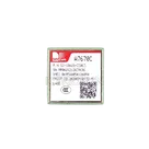
Part Data Audit and Verification

Looking at the datasheet of this component, can you group together pins by their functions? for example for Power, 3v3, gnd_1 gnd_2 etc
Also can you place them into their respective sections based on their functions
NOTE: If you group them, can you not add the same pin if you already added them in a group? You should know which pin function is common for its function
Worked for 13 sec
I’ll group each pin into exactly one functional section based on the A7670X R2 table, using Section for the block and Pin Group for the unique signal/rail subgroup (for example VBAT, VBUS, GND_1, GND_2, UART, USB).
Worked for 3 mins 33 sec
Done. I assigned every A7670C-LASE pin to exactly one functional
Section and one Pin Group, using unique groups for repeated physical pads like VBAT_55/56/57, GND_02, GND_17, etc., so no pin is double-counted.I also corrected a few pin types from the newer A7670X R2 table and updated A7670C-LASE Part Audit with the grouping scheme and validation result.
Create visual grouping
Verify footprint mapping
Add section documentation
Review naming consistency
Export pin table
Refine this doc
Ask about this doc
A7670C-LASE Part Audit
Scope
Reviewed the current Flux part project for SIMCom A7670C-LASE against available official/public part information: MPN, package, pin count, description, project properties, schematic symbol terminals, and PCB footprint pad count.
Current Flux Part Metadata
Table
| Field | Current value |
|---|---|
| Project / part name | A7670C-LASE |
| Manufacturer Part Number | A7670C-LASE |
| Manufacturer | SIMCOM(芯讯通无线科技) |
| LCSC Part Number | C2888406 |
| JLCPCB Part Class | Extended Part |
| Designator Prefix | U |
| Package / case | LGA-124_L24.0-W24.0-P1.0-A7670C-LASS |
| Symbol terminals | 124 terminal components |
| Footprint pads | 124 PCB pads |
| Existing Datasheet URL before audit | Not present |
Datasheet / Source URL Update
I could not retrieve a direct official PDF URL from SIMCom's site, but the official SIMCom A7670X product page exposes the relevant download entry:
- Official product/download page set as Datasheet URL: https://cn.simcom.com/product/A7670X.html
- Latest matching official document listed there:
A7670X R2硬件设计手册_V1.14, updated 2026-03-18. - Related official legacy document:
A7670C_R2_硬件设计手册_V1.06.
The project property
Datasheet URL was added with the SIMCom product/download page. Implementation Details, Domain, Connectivity, and nominal Operating Voltage were also updated.Key Specs Found
Table
| Spec | Datasheet / official-source value |
|---|---|
| Module family | A7670X / A7670C R2 cellular module |
| Variant group | A7670C includes LASE / LASC variants |
| Cellular category | LTE Cat 1; GSM support also listed |
| A7670C-LASE bands | EGSM900, DCS1800, LTE-FDD B1/B3/B5/B8, LTE-TDD B34/B38/B39/B40/B41 |
| Package style | LGA + LCC module |
| Package/pin count | 124 pins: 80 outer LCC pins + 44 inner LGA pins |
| Dimensions | 24.0 mm × 24.0 mm; height about 2.3 to 2.4 mm depending source/version |
| Nominal VBAT | 3.8 V |
| VBAT operating range | 3.4 V to 4.2 V |
| USB VBUS operating range | 3.0 V to 5.4 V, 5.0 V typical |
| Peak supply current | Up to about 2 A during transmit bursts; supply should support >=2 A and keep droop <300 mV |
| Interfaces | USB, UART, debug UART, SPI, I2C/CI2C, GPIO, ADC, USIM1, USIM2, LCD, audio, GNSS, camera-related pins |
| RF pins | RF_ANT, GNSS_ANT, BT_ANT |
Symbol / Pin Cross-Check Summary
The Flux symbol has the correct total pin count (124) and most functional groups are present. However, many terminal names are aliases or generic GPIO names rather than the primary names in the A7670X R2 hardware-design pin table. All terminal
Pin Type values are currently Unspecified, and terminal-level Pin Description properties are absent, so the symbol is not fully datasheet-enriched.Exact / acceptable matches
The following critical pins match exactly or are obvious naming equivalents:
- PWRKEY pin 1
- GND pins 2, 17, 18, 29, 39, 45, 46, 54, 58, 59, 61-65, 69-89, 91, 92, 94
- TXD pin 9, RXD pin 10
- SPI_CLK pin 11, SPI_CS pin 12, SPI_MOSI pin 13, SPI_MISO pin 14
- RESET pin 16
- VBUS pin 24, ADC pin 25, USB_DP pin 27, USB_DM pin 28
- USIM1_VDD/DATA/CLK/RST/DET pins 30-34
- EAR_P/EAR_N pins 40/41, MIC_P/MIC_N pins 42/43
- UART3_RXD/TXD pins 49/50
- VBAT_ADC pin 51
- VBAT pins 55/56/57
- RF_ANT pin 60, GNSS_ANT pin 90, BT_ANT pin 93
- GNSS_TXD/RXD pins 95/96, GNSS_PWRCTL pin 98, 1PPS pin 100
- USIM2_DATA/CLK/VDD/RST/DET pins 108-112
- NC pins 113/114/115
- GNSS_VBKP pin 116
Name mismatches / aliases to review
Table
| Pin | Flux terminal name | Datasheet primary name | Assessment |
|---|---|---|---|
| 3 | AP_WAKEUP | DTR | Mismatch; AP_WAKEUP may be a function/alias but not the primary pin-table name. |
| 4 | GPIO_00 | RI | Mismatch. |
| 5 | GPIO_01 | DCD | Mismatch. |
| 6 | GPIO_02 | USB_BOOT | Mismatch; USB_BOOT is important for boot behavior. |
| 7 | GPIO_03 | CTS | Mismatch. |
| 8 | GPIO_04 | RTS | Mismatch. |
| 15 | VDD_1V8 | VDD_EXT | Naming mismatch; likely same external 1.8 V output, but datasheet primary name should be used or described. |
| 19 | GPIO_05 | GPIO1 | Numbering mismatch. |
| 20 | GNSS_PWR_EN/MK_IN_3 | MK_IN_3 | Extra GNSS_PWR_EN alias; verify variant-specific function. |
| 21 | GPIO_07/MK_OUT_3 | MK_OUT_3 | Extra GPIO alias; primary name differs. |
| 22 | UART_LOG_RX | DEBUG_RXD | Naming mismatch / likely equivalent debug UART receive. |
| 23 | UART_LOG_TX | DEBUG_TXD | Naming mismatch / likely equivalent debug UART transmit. |
| 26 | GPIO_17 | GPIO2 | Numbering mismatch. |
| 35 | GPIO_13/MK_OUT_6 | MK_OUT_6 | Extra GPIO alias; primary name differs. |
| 36 | GPIO_14/MK_IN_6 | MK_IN_6 | Extra GPIO alias; primary name differs. |
| 37 | I2C_SDA | CI2C_SDA | Naming mismatch; datasheet uses CI2C_SDA. |
| 38 | I2C_SCL | CI2C_SCL | Naming mismatch; datasheet uses CI2C_SCL. |
| 44 | GPIO_15/MK_OUT_2 | MK_OUT_2 | Extra GPIO alias; primary name differs. |
| 47 | GPIO_16/MK_IN_2 | MK_IN_2 | Extra GPIO alias; primary name differs. |
| 48 | GPIO_08 | GPIO3 | Numbering mismatch. |
| 52 | GPIO_09 | NETLIGHT | Mismatch; NETLIGHT is a named status output. |
| 53 | GPIO_18 | GPIO4 | Numbering mismatch. |
| 66 | GPIO_10 | STATUS | Mismatch; STATUS is a named status output. |
| 67 | GPIO_11/MK_OUT_5 | MK_OUT_5 | Extra GPIO alias; primary name differs. |
| 68 | GPIO_12/MK_IN_5 | MK_IN_5 | Extra GPIO alias; primary name differs. |
| 97 | 1V8_GNSS | VDD_GNSS | Naming mismatch; datasheet primary name is VDD_GNSS. |
| 99 | VDD_2V8 | VDD_AUX | Naming mismatch; verify voltage/function. |
| 101 | GPIO_19/LCD_BL_PWM | LCD_BL_PWM | Extra GPIO alias; primary name differs. |
| 102 | GPIO_20/LCD_SPI_CLK | LCD_SPI_CLK | Extra GPIO alias; primary name differs. |
| 103 | GPIO_21/LCD_SPI_TXD | LCD_SPI_TXD | Extra GPIO alias; primary name differs. |
| 104 | GPIO_22/LCD_SPI_RXD | LCD_SPI_RXD | Extra GPIO alias; primary name differs. |
| 105 | GPIO_23/LCD_SPI_CS | LCD_SPI_CS | Extra GPIO alias; primary name differs. |
| 106 | GPIO_24/LCD_RST | LCD_RST | Extra GPIO alias; primary name differs. |
| 107 | GPIO_25/LCD_DCX | LCD_DCX | Extra GPIO alias; primary name differs. |
| 117 | GPIO_26 | CAM_I2C_SDA | Mismatch. |
| 118 | GPIO_27 | CAM_I2C_SCL | Mismatch. |
| 119 | GPIO_28 | CAM_PWDN | Mismatch. |
| 120 | GPIO_29 | CAM_RST | Mismatch. |
| 121 | GPIO_30 | CAM_MCLK | Mismatch. |
| 122 | GPIO_31 | CAM_SPI_D0 | Mismatch. |
| 123 | GPIO_32 | CAM_SPI_D1 | Mismatch. |
| 124 | GPIO_33 | CAM_SPI_CLK | Mismatch. |
Footprint Cross-Check
Table
| Check | Result |
|---|---|
| Pad count | Pass: 124 pads found, matching A7670X R2 124-pin package. |
| Package size | Generally consistent with 24 mm × 24 mm module family. |
| Package style | Project package text says LGA-124, while datasource describes LGA+LCC with 80 outer LCC + 44 inner LGA pins. Recommend renaming package metadata to reflect LGA+LCC/LCC-124 style. |
| Pad geometry | Sampled pads show outer-edge rectangular/circular pads and inner square pads consistent with mixed LCC/LGA layout style, but a full dimensional audit against Figure 3/4 requires direct mechanical drawing access. |
| Copper layer setup | Layout summary reports 0 copper layers in the part-project board setup, which is typical/irrelevant for a footprint asset but should not be interpreted as an application PCB stackup. |
Flagged Issues
- Datasheet URL was missing — fixed by setting the official SIMCom product/download page.
- Symbol terminal names are not consistently datasheet-primary names — several pins use GPIO-number aliases or product-specific aliases instead of the A7670X R2 hardware manual names.
- Pin descriptions are missing — no terminal-level
Pin Descriptionproperties were found. - Pin electrical types are all
Unspecified— power, ground, input, output, bidirectional, analog, RF, and NC pins should be typed for better ERC and downstream usability. - Package metadata is slightly ambiguous — current package says
LGA-124..., while official/public data describes the R2 module asLGA+LCC, 124 pins, 80 outer LCC + 44 inner LGA.
Recommended Fixes
- Update terminal names to datasheet primary names, or add datasheet-primary names in
Pin Descriptionif aliases are intentionally preserved. - Add
Pin Descriptionfor every terminal from the A7670X R2 hardware-design pin description table. - Set
Pin Typefor each terminal group:- Power input: VBAT, VBUS
- Power output/reference: VDD_EXT/VDD_1V8, VDD_GNSS, VDD_AUX/2V8, USIM supplies
- Ground: all GND pins
- RF: RF_ANT, GNSS_ANT, BT_ANT
- Digital I/O: UART, SPI, I2C/CI2C, GPIO, LCD, camera, USIM signals
- Analog/audio: ADC, VBAT_ADC, MIC_P/N, EAR_P/N
- NC: pins 113-115
- Rename or clarify package metadata to
LGA+LCC-124_24x24mm_P1.0_A7670C_R2or similar. - If exact dimensional verification is required, download the official
A7670X R2硬件设计手册_V1.14from SIMCom and compare every pad coordinate/size against Figures 3 and 4.
Fix Applied — 2026-06-03
The symbol terminal metadata has been updated against the A7670X R2 pin definition table:
- Renamed all alias/non-primary terminal names to the A7670X R2 primary pin names.
- Added datasheet-based
Pin Descriptionvalues for all 124 terminals. - Set
Pin Typeto Flux-standard electrical types mapped from the datasheet codes:- DI / AI → Input
- DO / AO → Output
- DIO / AIO → Bi-Directional
- PI → Power In
- PO → Power Out
- GND → Ground
- NC → Not Connected
- Added the project-level
Part TypevalueRF Transceiverto clear the remaining part-review metadata warning.
Post-fix validation: component review checks for terminals, terminal parametrics, terminal pin numbers, and missing properties returned no ERROR/WARNING/UNCERTAIN results.
Fix Applied — Functional Pin Grouping — 2026-06-03
Pins were organized into exactly one functional
Section each, with Pin Group used for the local bus/rail subgroup. No pin was intentionally duplicated across multiple functional sections.Grouping scheme applied:
Table
| Section | Pin groups used | Notes |
|---|---|---|
| Power Rails | VBAT_55, VBAT_56, VBAT_57, 1V8_OUTPUT, 3V0_OUTPUT | Main battery input pins are kept as separate physical groups to avoid double-counting high-current pads. |
| Ground | GND_02, GND_17, GND_18, GND_29, GND_39, GND_45, GND_46, GND_54, GND_58, GND_59, GND_61–GND_65, GND_69–GND_89, GND_91, GND_92, GND_94 | Each GND pad is uniquely grouped by pin number. |
| Power Control | PWRKEY | Power on/off control input. |
| Boot and Reset | USB_BOOT, RESET | Boot/download and hardware reset pins. |
| Main UART | UART0_DATA, UART0_FLOW, UART0_MODEM | TXD/RXD, RTS/CTS, DTR/RI/DCD. |
| Debug UART | DEBUG_UART | DEBUG_RXD / DEBUG_TXD. |
| UART3 | UART3 | UART3_RXD / UART3_TXD. |
| SPI Interface | SPI | SPI_CLK / CS / MOSI / MISO. |
| USB | USB_VBUS, USB_DP_DM | VBUS and USB 2.0 differential pair. |
| USIM1 | USIM1_POWER, USIM1_SIGNAL, USIM1_DETECT | USIM1 supply, data/clock/reset, and detect. |
| USIM2 | USIM2_POWER, USIM2_SIGNAL, USIM2_DETECT | USIM2 supply, data/clock/reset, and detect. |
| I2C | CI2C | CI2C_SDA / CI2C_SCL. |
| GPIO | GPIO | GPIO1–GPIO4 only. Other multifunction pins were grouped by their primary datasheet function instead of GPIO alias. |
| Keypad Matrix | KEYPAD_IN, KEYPAD_OUT | MK_IN_x and MK_OUT_x pins. |
| Audio | EARPHONE_OUT, MIC_INPUT | Differential earpiece output and microphone input. |
| Analog and Status | ADC, VBAT_ADC, STATUS_INDICATORS | ADC inputs plus NETLIGHT/STATUS outputs. |
| RF Antennas | MAIN_RF_ANT, GNSS_ANT, BT_ANT | Main cellular, GNSS, and Bluetooth antenna interfaces. |
| GNSS | GNSS_POWER, GNSS_BACKUP_POWER, GNSS_UART, GNSS_CONTROL, GNSS_TIMING | GNSS supply/control/serial/1PPS pins. |
| LCD Interface | LCD_SPI, LCD_CONTROL | LCD SPI pins, reset, DCX, and backlight PWM. |
| Camera Interface | CAM_I2C, CAM_CONTROL, CAM_CLOCK, CAM_SPI | Camera I2C/control/MCLK/SPI pins. |
| No Connect | NC_113, NC_114, NC_115 | Each NC pad is separately identified and kept in the No Connect section. |
Corrections made during grouping:
VBUSpin type set toPower In.VDD_GNSSset toPower Inper the A7670X R2 table.GNSS_PWRCTLset toInputper the A7670X R2 table.LCD_SPI_TXD,CAM_SPI_D0, andCAM_SPI_D1set toBi-Directionalwhere the table indicates DIO/bidirectional function.GNSS_ANTset toBi-Directionalto match the antenna interface behavior.
Post-grouping validation: sampled terminals show the expected
Section and Pin Group assignments, and component review checks for terminal metadata still return no ERROR/WARNING/UNCERTAIN results.Scope
Current Flux Part Metadata
Datasheet / Source URL Update
Key Specs Found
Symbol / Pin Cross-Check Summary
Exact / acceptable matches
Name mismatches / aliases to review
Footprint Cross-Check
Flagged Issues
Recommended Fixes
Fix Applied — 2026-06-03
Fix Applied — Functional Pin Grouping — 2026-06-03