3D Camera Module Project Overview
Thought for 1 min 26 sec
Here’s a detailed explanation of the project:
Overall Purpose
The project is a 3D Camera Module designed for scalable photogrammetry reconstruction. Its main objective is to capture synchronized images from multiple cameras (organized in an array) so that they can later be combined into 3D models. By using a modular architecture, additional camera modules can be linked together to expand the system’s capacity while preserving timing and capture synchronization.
Core Components and Their Roles
-
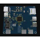
Camera Array (4-Camera Array):
- Function: Provides multiple viewpoints for 3D photogrammetry by capturing images from slightly different angles.
- Interaction: Each camera module is designed to work in sync with the others through a unified control interface.
-
Microcontroller (ATMEGA32U4):
- Function: Acts as the central processing unit that manages camera operations. It provides built-in USB 2.0 for data transfer, handles digital adjustments and timing, and controls synchronization sequences.
- Interaction: Communicates with the camera modules over SPI for high-speed image data transfer. It also drives the logic for capturing commands and timing adjustments.
-
SPI Communication Interface:
- Function: Facilitates high-speed data transfer from each camera module to the microcontroller.
- Interaction: The SPI bus connects the individual cameras to the master controller (the ATMega32U4), ensuring that image data is captured in a synchronized manner.
-
I2C Bus:
- Function: Provides a secondary communication link that connects the camera modules together.
- Interaction: The I2C bus is used to share configuration and synchronization data between modules, ensuring that capture sequences remain coordinated across the array.
-
USB 2.0 Interface:
- Function: Enables data transfer from the microcontroller to an external host (such as a computer) for further processing or image review.
- Interaction: It is used primarily for configuration, data transfer, and debugging after the sensor data is collected.
-
Micro SD Card Slot:
- Function: Provides local storage for captured images in situations where immediate USB streaming is not feasible.
- Interaction: The microcontroller writes data to the SD card for logging or buffering images, which can later be read for post-processing.
-
Power Supply Options:
- USB-C (5V): Offers a common power source that is easy to use and ubiquitous in modern devices.
- Barrel Jack (12V Regulated to 5V): Gives an alternative power input if a higher voltage supply is available; this is internally regulated down to 5V for the digital circuitry.
-
Interrupt Logic Pin on SPI Master:
- Function: Provides a dedicated signal to trigger capture events.
- Interaction: When the master module receives an interrupt (for example, from an external command), it initiates a synchronous capture across all camera modules.
Design, Implementation, and Functionality Breakdown
-
Modular and Scalable Design:
- The system is built as a module that can be connected with others. Each module communicates via the I2C bus so that even when multiple units are connected, the capture timing remains in sync.
- The use of standard interfaces (SPI for high-speed data and I2C for control) allows for flexibility and scalability.
-
Data Flow and Processing:
- Capture Phase: When a capture command is issued (via the interrupt pin), all connected cameras capture their images simultaneously.
- Data Transfer: The images are sent via SPI to the ATMega32U4, which then either transfers the data over USB to a host or saves it locally on the micro SD card.
- Communication: The I2C connection ensures that configuration data (like exposure settings) and trigger timing are consistent across the camera array.
-
Power and Signal Conditioning:
- The board design accepts dual power inputs with appropriate regulation. This allows the design to function with either a 5V USB-C supply or a 12V input (after regulation) ensuring stable operation.
- Decoupling and other passive component choices (such as resistors and capacitors referenced in the project schematic) support stable operation in a high-speed digital environment.
-
Synchronization and Control:
- The microcontroller’s firmware must manage both SPI and I2C communication effectively to balance high-speed data transfer with precise timing control.
- Special attention is given to the interrupt and trigger logic to minimize lag between modules, a critical factor for successful 3D reconstruction.
Key Technologies and Design Choices
-
SPI and I2C Communication:
The use of these two protocols is a common design choice in multi-module systems. SPI offers the necessary bandwidth for image data, while I2C simplifies configuration and synchronization tasks. -
ATMEGA32U4 Microcontroller:
Selected for its built-in USB support and sufficient processing power for handling multiple camera streams as well as peripheral management. -
USB 2.0 Interface:
While USB 2.0 provides adequate speeds for many applications, it can be a limiting factor for continuous high-speed image streaming. This design choice is a trade-off between cost, complexity, and performance. -
Dual Power Supply Options:
Offering both USB-C and barrel jack inputs increases the versatility of the system, making it easier to integrate into different environments.
Potential Challenges and Considerations
-
Synchronization Across Modules:
Achieving perfect synchronization during capture can be challenging. Signal delays and bus latency (especially on I2C) must be carefully managed. -
Data Bandwidth:
Transferring high-resolution images over SPI and then through USB 2.0 could saturate the available bandwidth, potentially leading to bottlenecks. Buffering on the SD card is one strategy to mitigate this. -
Power Stability:
The mixed power input approach requires robust regulation and filtering to minimize noise, which is especially critical for image sensor performance. -
Firmware Complexity:
The code managing multiple high-speed data interfaces must be highly optimized and bug-free, or else the synchronized capture may be compromised. -
Design Trade-offs:
- Cost vs. Performance: Choosing a microcontroller like the ATMega32U4 helps keep costs down, but it might not have the processing headroom that a more powerful MCU would offer.
- Interface Limitations: USB 2.0 is adequate for many scenarios but may require alternative approaches (such as using SD card buffering) for higher data loads.
Real-World Applications and Future Enhancements
-
Applications:
- 3D Reconstruction and Photogrammetry: Enabling accurate 3D modeling for applications such as virtual reality, architecture, and industrial inspection.
- Multi-Camera Surveillance: Synchronized image capture across various angles could improve smart surveillance systems.
- Robotics and Navigation: Stereo or multi-view systems can be used for depth sensing in autonomous vehicles and drones.
-
Areas for Improvement:
- Enhanced Throughput: Investigate moving to USB 3.0 or incorporating higher performance microcontrollers for increased data throughput.
- Improved Synchronization: Use additional hardware triggers or even FPGA-based controllers to ensure even tighter capture synchronization.
- Optimized Power Management: Explore more efficient power conversion and regulation techniques to reduce noise and improve reliability.
- Scalability: Further modularize the design to seamlessly integrate more cameras without significant redesign, perhaps by incorporating smarter bus arbitration strategies.
This breakdown should give you a comprehensive view of the project’s design, how key components interact, and the main considerations involved in building and potentially enhancing the system.
Main design goals
Sync challenges
Data management
Power considerations
Long-term improvements