Part Information Review and Mismatch Check
5:23
Evalu.
Checking.
Extract.
Analy.
Using Schematic Tool.
Using PCB Layout Tool.
Using PCB Layout Tool.
Looking for "Features list for TQ2 series relays" in mech_eng_tq.pdf
Looking for "Part numbering system and types including TQ2-L2 and coil voltage options" in mech_eng_tq.pdf
Looking for "Contact arrangement and rating (2 Form C, 2 A) for TQ2 series" in mech_eng_tq.pdf
Looking for "Coil data for latching dual coil type 4.5 V nominal voltage" in mech_eng_tq.pdf
Looking for "Must operate voltage and must release voltage for TQ2-L2-4.5V" in mech_eng_tq.pdf
Looking for "Nominal operating power for latching type TQ2 series" in mech_eng_tq.pdf
Looking for "Maximum switching voltage and maximum switching current for TQ2 series" in mech_eng_tq.pdf
Looking for "Minimum switching load for TQ2 series" in mech_eng_tq.pdf
Looking for "Insulation resistance and dielectric strength specifications" in mech_eng_tq.pdf
Looking for "Operate time and release time for latching type" in mech_eng_tq.pdf
Looking for "Electrical life and mechanical life ratings" in mech_eng_tq.pdf
Looking for "Ambient temperature operating range and storage temperature range" in mech_eng_tq.pdf
Looking for "Dimensions drawing for TQ2 package (mm) height 5 mm" in mech_eng_tq.pdf
Looking for "Terminal arrangement and internal connections (bottom view) for dual coil latching TQ2-L2" in mech_eng_tq.pdf
Looking for "Recommended PC board pattern (land pattern) for TQ2 through hole type" in mech_eng_tq.pdf
Looking for "Soldering conditions for through hole type" in mech_eng_tq.pdf
Looking for "Weight specification for TQ2 series" in mech_eng_tq.pdf
Looking for "Contact material and contact resistance spec" in mech_eng_tq.pdf
Looking for "Pin numbering for TQ2-L2 and mapping to COM, NO, NC, coil pins" in mech_eng_tq.pdf
Looking for "Dual coil latching terminal arrangement bottom view with polarity marks for coil pins for TQ2-L2 (pins 1,6,7,10 indicated +/−)" in mech_eng_tq.pdf
Looking for "Terminal numbering and contact assignment mapping COM1, NO1, NC1, COM2, NO2, NC2 to pin numbers for TQ2-L2" in mech_eng_tq.pdf
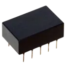
- Part: TQ2-L2-4.5V
- Manufacturer: Panasonic
- Description: Flat, 5 mm 2 Form C, 2 A, relays
- Designator prefix: K
- Datasheet: https://industry.panasonic.com/ac/cdn/e/control/relay/signal/catalog/mech_eng_tq.pdf
- Schematic symbol pins present: 10 total
- Asset: KiCad footprint “TQ2L245V.kicad_mod”
- Pads (through-hole) count: 10, arranged 5 x 2
- Pad coordinates: 1–5 at y=0.00 mm; 6–10 at y=−7.62 mm; x-spacing 0, 2.54, 5.08, 7.62, 10.16 mm
- Drill size: 1.0 mm
- Datasheet URL already set on the part. No web search or property update needed.
- Three terminal styles: PC board terminal (standard/self-clinching), surface-mount terminal
- Conforms to FCC Part 68: surge withstand 1,500 V (between open contacts)
- M.B.B. contact available
- SMD types conform to JIS C0806
- TQ2-L2-4.5V = TQ series, “2” = 2 Form C, “L2” = 2-coil latching, “4.5V” coil
- DC coil voltages offered: 1.5 (SMD only), 3, 4.5, 5, 6, 9, 12, 24, 48 V (48 V only single side stable)
- Contact arrangement: 2 Form C
- Contact rating (resistive): 2 A 30 V DC, 0.5 A 125 V AC
- Max. switching voltage: 220 V DC, 125 V AC
- Max. switching current: 2 A (DC/AC)
- Set voltage (20°C): ≤ 75% of nominal
- Reset voltage (20°C): ≤ 75% of nominal
- Nominal operating current (20°C): Set coil 44.4 mA; Reset coil 44.4 mA
- Coil resistance (±10%, 20°C): Set 101.2 Ω; Reset 101.2 Ω
- Nominal operating power: 200 mW (each coil)
- Max. applied voltage (20°C): 150% of nominal
- Insulation/dielectric specifications are present in the catalog, but portions of the PDF intermittently failed to fetch; recommend confirming exact dielectric test voltages on the PDF page if needed for compliance documentation.
- Mechanical life: Min. 100 × 10^6 operations (180 ops/min)
- Electrical life (2 Form C, resistive, 20 ops/min): typical entries include 1 A 30 V DC ≥ 200 × 10^3 ops; 2 A 30 V DC ≥ 100 × 10^3 ops; 0.5 A 125 V AC ≥ 100 × 10^3 ops
- Latching timing sections (operate/reset) present in catalog
- Ambient operating temperature: −40 to +85 °C (over 70 °C: Max. 1 A)
- Recommended PC board pattern (bottom view): 2.54 mm pin pitch, 7.62 mm row spacing, 10 holes, φ1.0 mm, tolerance ±0.1 mm
- Dimensions drawing is in the catalog (fetch intermittently failed); headline series height is 5 mm
- 2-coil latching (Reset) polarity marks at pins: 1 = +, 6 = −, 7 = +, 10 = −
- Contact-to-pin mapping (PC board terminal style):
- COM1 → pin 2
- NO1 → pin 3
- NC1 → pin 4
- COM2 → pin 9
- NO2 → pin 8
- NC2 → pin 7
Table
| Pin | Project symbol | Datasheet function | Match |
|---|---|---|---|
| 1 | COIL_ | Coil + (latching coil, polarity +) | OK |
| 2 | NC_1 | COM1 | MISMATCH (project labels NC1; should be COM1) |
| 3 | COM_1 | NO1 | MISMATCH (project labels COM1; should be NO1) |
| 4 | NO_1 | NC1 | MISMATCH (project labels NO1; should be NC1) |
| 5 | COIL-_1 | Contact row (not a coil pin) | MISMATCH (project labels coil −; datasheet shows coil − at pin 6/10) |
| 6 | COIL-_2 | Coil − (paired with pin 1) | POLARITY/FUNCTION MISMATCH in name (this is coil − for the pin‑1 coil; project labels it as coil 2 −) |
| 7 | NO_2 | NC2 | MISMATCH (project labels NO2; should be NC2) |
| 8 | COM_2 | NO2 | MISMATCH (project labels COM2; should be NO2) |
| 9 | NC_2 | COM2 | MISMATCH (project labels NC2; should be COM2) |
| 10 | COIL | Coil − (polarity − for the second coil) | MISMATCH (project labels +; datasheet shows −) |
- Contact function mapping is rotated for both poles:
- Pins 2–4 should be COM1–NO1–NC1 (project has NC1–COM1–NO1).
- Pins 7–9 should be NC2–NO2–COM2 (project has NO2–COM2–NC2).
- Coil polarity and identification:
- Pin 1 is correctly “+”; its paired “−” is pin 6. The project has COIL-_1 on pin 5 and COIL-_2 on pin 6, implying the wrong coil assignment.
- Pin 10 should be coil “−” (for the other coil), but the project labels COIL there.
- The naming COIL_ vs COIL is ambiguous; prefer explicit “SET+ / SET− / RESET+ / RESET−” or “COIL1+/−, COIL2+/−” per datasheet polarity marks.
- Pin count: 10 — matches.
- Grid: 2.54 mm pitch across each row — matches.
- Row spacing: 7.62 mm — matches.
- Drill: 1.0 mm — matches recommended φ1.0 mm holes.
- Footprint outline present and consistent with recommended keepouts (from KiCad mod). No obvious footprint dimension red flags detected.
- The current symbol pin mapping and coil polarity labeling do not match the datasheet. As-is, this will cause incorrect wiring and functional failure on the assembled board, even though the physical footprint geometry matches the recommended land pattern.
- Footprint geometry aligns with the datasheet pattern (pitch, row spacing, drill), so manufacturing fit is likely OK; the critical issue is the symbol pin/function mapping.
Ready.
Reviews

- Wirelessly connects nets on schematic. Used to organize schematics and separate functional blocks. To wirelessly connect net portals, give them same designator. #portaljharwinbarrozo43.0M
- Wirelessly connects power nets on schematic. Identical to the net portal, but with a power symbol. Used to organize schematics and separate functional blocks. To wirelessly connect power net portals, give them the same designator. #portal #powerjharwinbarrozo11.4M
- A generic fixed resistor for rapid developing circuit topology. Save precious design time by seamlessly add more information to this part (value, footprint, etc.) as it becomes available. Standard resistor values: 1.0Ω 10Ω 100Ω 1.0kΩ 10kΩ 100kΩ 1.0MΩ 1.1Ω 11Ω 110Ω 1.1kΩ 11kΩ 110kΩ 1.1MΩ 1.2Ω 12Ω 120Ω 1.2kΩ 12kΩ 120kΩ 1.2MΩ 1.3Ω 13Ω 130Ω 1.3kΩ 13kΩ 130kΩ 1.3MΩ 1.5Ω 15Ω 150Ω 1.5kΩ 15kΩ 150kΩ 1.5MΩ 1.6Ω 16Ω 160Ω 1.6kΩ 16kΩ 160kΩ 1.6MΩ 1.8Ω 18Ω 180Ω 1.8KΩ 18kΩ 180kΩ 1.8MΩ 2.0Ω 20Ω 200Ω 2.0kΩ 20kΩ 200kΩ 2.0MΩ 2.2Ω 22Ω 220Ω 2.2kΩ 22kΩ 220kΩ 2.2MΩ 2.4Ω 24Ω 240Ω 2.4kΩ 24kΩ 240kΩ 2.4MΩ 2.7Ω 27Ω 270Ω 2.7kΩ 27kΩ 270kΩ 2.7MΩ 3.0Ω 30Ω 300Ω 3.0KΩ 30KΩ 300KΩ 3.0MΩ 3.3Ω 33Ω 330Ω 3.3kΩ 33kΩ 330kΩ 3.3MΩ 3.6Ω 36Ω 360Ω 3.6kΩ 36kΩ 360kΩ 3.6MΩ 3.9Ω 39Ω 390Ω 3.9kΩ 39kΩ 390kΩ 3.9MΩ 4.3Ω 43Ω 430Ω 4.3kΩ 43KΩ 430KΩ 4.3MΩ 4.7Ω 47Ω 470Ω 4.7kΩ 47kΩ 470kΩ 4.7MΩ 5.1Ω 51Ω 510Ω 5.1kΩ 51kΩ 510kΩ 5.1MΩ 5.6Ω 56Ω 560Ω 5.6kΩ 56kΩ 560kΩ 5.6MΩ 6.2Ω 62Ω 620Ω 6.2kΩ 62KΩ 620KΩ 6.2MΩ 6.8Ω 68Ω 680Ω 6.8kΩ 68kΩ 680kΩ 6.8MΩ 7.5Ω 75Ω 750Ω 7.5kΩ 75kΩ 750kΩ 7.5MΩ 8.2Ω 82Ω 820Ω 8.2kΩ 82kΩ 820kΩ 8.2MΩ 9.1Ω 91Ω 910Ω 9.1kΩ 91kΩ 910kΩ 9.1MΩ #generics #CommonPartsLibraryjharwinbarrozo1.5M
- A generic fixed capacitor ideal for rapid circuit topology development. You can choose between polarized and non-polarized types, its symbol and the footprint will automatically adapt based on your selection. Supported options include standard SMD sizes for ceramic capacitors (e.g., 0402, 0603, 0805), SMD sizes for aluminum electrolytic capacitors, and through-hole footprints for polarized capacitors. Save precious design time by seamlessly add more information to this part (value, footprint, etc.) as it becomes available. Standard capacitor values: 1.0pF 10pF 100pF 1000pF 0.01uF 0.1uF 1.0uF 10uF 100uF 1000uF 10,000uF 1.1pF 11pF 110pF 1100pF 1.2pF 12pF 120pF 1200pF 1.3pF 13pF 130pF 1300pF 1.5pF 15pF 150pF 1500pF 0.015uF 0.15uF 1.5uF 15uF 150uF 1500uF 1.6pF 16pF 160pF 1600pF 1.8pF 18pF 180pF 1800pF 2.0pF 20pF 200pF 2000pF 2.2pF 22pF 20pF 2200pF 0.022uF 0.22uF 2.2uF 22uF 220uF 2200uF 2.4pF 24pF 240pF 2400pF 2.7pF 27pF 270pF 2700pF 3.0pF 30pF 300pF 3000pF 3.3pF 33pF 330pF 3300pF 0.033uF 0.33uF 3.3uF 33uF 330uF 3300uF 3.6pF 36pF 360pF 3600pF 3.9pF 39pF 390pF 3900pF 4.3pF 43pF 430pF 4300pF 4.7pF 47pF 470pF 4700pF 0.047uF 0.47uF 4.7uF 47uF 470uF 4700uF 5.1pF 51pF 510pF 5100pF 5.6pF 56pF 560pF 5600pF 6.2pF 62pF 620pF 6200pF 6.8pF 68pF 680pF 6800pF 0.068uF 0.68uF 6.8uF 68uF 680uF 6800uF 7.5pF 75pF 750pF 7500pF 8.2pF 82pF 820pF 8200pF 9.1pF 91pF 910pF 9100pF #generics #CommonPartsLibraryjharwinbarrozo1.5M
- A generic fixed inductor for rapid developing circuit topology. *You can now change the footprint and 3D model at the top level anytime you want. This is the power of #genericsjharwinbarrozo15.6k
- An electrical connector acting as reusable interface to a conductor and creating a point where external circuits can be connected.Terminal
- 47 kOhms ±5% 0.125W, 1/8W Chip Resistor 0805 (2012 Metric) Automotive AEC-Q200 Thick Film #forLedBlinkjharwinbarrozo1.2M
- 10uF Capacitor Aluminum Polymer 20% 16V SMD 5x5.3mm #forLedBlink #commonpartslibrary #capacitor #aluminumpolymer #radialcanjharwinbarrozo1.2M
- Yellow 595nm LED Indication - Discrete 1.7V 1206 (3216 Metric) #forLedBlinkjharwinbarrozo1.1M


Pricing & Availability
See prices from popular manufacturers for your project.
Assets

TQ2-L2-4.5V
TQ2-L2-4.5V Symbol.svgDefaultTQ2-L2-4.5V
TQ2L245V.kicad_modFootprintTQ2-L2-4.5V
TQ2-L2-4.5V.stp3D Model
TQ2-L2-4.5V-thumb.png
TQ2-L2-4.5V-thumbThumbnailControls
Welcome 👋
Flux accelerates your PCB design with AI.
Create your account to start using this component and bring your ideas to life.