Chat

Welcome to Flux

Treat Flux like your intern. Tell it what you'd like to build and it'll get to work. You can also ask it questions, brainstorm ideas, and teach it your preferences. Learn More
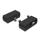
Explain this part
Write a part description
Describe each pin
Operating conditions
Electrical max ratings
Part Specifications
Application circuits
Verify Part Details
Recommend similar parts
Check availability & lifecycle
create a detailed step by step plan table for this project to verify its functio...

@copilot create a detailed step by step plan table for this project to verify its functionality.
1y
Certainly! Here's a step-by-step plan to verify the functionality of your circuit using the S8050 NPN BJT transistor:

Table


StepTaskInstructions
1Component IdentificationEnsure that you have all the required components: S8050 transistor, and possibly resistors, capacitors, etc.
2Initial SetupOpen your project in Flux. Place the transistor on the canvas. Ensure Q1 is the identifier for the S8050.
3Pin IdentificationIdentify the transistor pins: B (Base), C (Collector), E (Emitter).
4Base ConnectionConnect B to a suitable bias resistor (say $R_1$) to control the transistor. Connect $R_1$:2 to B:1
5Collector SetupConnect C to the load (e.g., $R_2$). Connect $R_2$:1 to C:1
6Emitter ConnectionConnect E to the ground node. Connect E:1 directly to ground.
7Power SupplyApply a suitable DC voltage to the circuit: Vcc to one end of $R_2$. Vcc to $R_2$:2
8Simulation ConfigurationConfigure a basic DC analysis or transient analysis in Flux to verify that the circuit works as expected.
9Run SimulationRun the simulation and observe the current flow. Verify that the transistor is operating in the desired region.
10Check Voltage LevelsUse measurement tools to check the voltages at Base, Collector, and Emitter to ensure proper biasing.
11Iterate and ModifyIf necessary, iterate and modify resistor values to achieve desired current and voltage levels.
12Document and ConcludeOnce functionality is verified, document the results and any changes made for future reference.
Detailed Connections
  • Base Biasing:
    • Connect $R_1$:2 to B:1. The other end of $R_1$, $R_1$:1, will be connected to a voltage source (bias supply).
  • Load:
    • Connect $R_2$:1 to C:1.
    • Connect $R_2$:2 to the Vcc (positive voltage supply).
  • Emitter to Ground:
    • Connect E:1 to GND.
Assumptions
  • Biasing Resistor $R_1$: Let's assume a typical value of 10kΩ.
  • Load Resistor $R_2$: Let's assume a typical value of 1kΩ.
  • Supply Voltage (Vcc): Let's assume 5V for initial testing.
Feel free to adjust the values based on your specific requirements and feedback from the simulation results. If you have any specific assumptions or component values, do let me know!
1y
Someone is typing...
2
E
C
B


S8050

S8050 thumbnail
Bipolar (BJT) Transistor NPN 25V 500 mA 150MHz 300 mW Surface Mount SOT-23 #commonpartslibrary #transistor #bjt

Properties

Transistor

MDD

S8050

Q

Pricing & Availability

Distributor

Qty 1

Controls