Part Information Review and Verification
Thought for 1 min 19 sec
I reviewed the part metadata, symbol terminals, and footprint against the official Renesas datasheet, using the datasheet as the source of truth as recommended for part-project verification
Summary
- The
Datasheet URLproperty is already set, so I did not search the web or change that property. - The part is broadly identified correctly as a Renesas buck-boost IC.
- The main metadata mismatch is the package property:
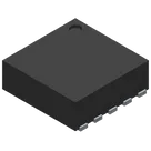
- Project: Package or Case Code =
TO - Datasheet: 10 Ld DFN, 0.5 mm pitch, L10.2.5x2.5
- Project: Package or Case Code =
- The symbol terminal count matches the datasheet:
- Datasheet: 10 leads + exposed pad
- Project: 11 terminals total, including EPAD
- The terminal names and pin numbers match the datasheet.
- The biggest symbol-data gap is that all terminals are currently
Pin Type: Unspecifiedand there are no pin descriptions. For a part-project audit, those should be populated from the datasheet rather than left blank
Table
| Field | In project | Datasheet / official source | Status |
|---|---|---|---|
| Manufacturer Part Number | RAA2361052GNP#HC5 | RAA2361052GNP#HC5 | Match |
| Manufacturer Name | Renesas | Renesas Electronics | Acceptable |
| Part Type | Integrated Circuits | Ultra-low IQ buck-boost regulator with bypass | Acceptable but generic |
| Designator Prefix | IC | Not a datasheet mismatch, but nonstandard vs common U usage | Not critical |
| Package or Case Code | TO | 10 Ld DFN, 0.5 mm pitch, L10.2.5x2.5 | Mismatch |
| Datasheet URL | Present | Official Renesas page/datasheet available | Match |
Table
| Parameter | Value |
|---|---|
| Function | Ultra-low IQ buck-boost regulator with bypass |
| Input voltage | 1.8 V to 5.5 V |
| Output voltage | 1.8 V to 5.0 V |
| Output current | Up to 400 mA |
| Input quiescent current | 130 nA |
| Peak efficiency | 96% |
| Operating temperature | -40°C to +85°C |
| Package | 10 Ld DFN, 0.5 mm pitch, L10.2.5x2.5 |
| Exposed pad | Yes; must be soldered to GND |
Datasheet pinout says:
Table
| Pin | Name | Function | Project status |
|---|---|---|---|
| 1 | EN | Enable input | Match |
| 2 | RSVD | Reserved, pull to GND | Match |
| 3 | BYPASS | Forced bypass control | Match |
| 4 | ILIM | Input current limit reader | Match |
| 5 | VSET | Output voltage reader | Match |
| 6 | VOUT | Output | Match |
| 7 | LX2 | Boost switch node | Match |
| 8 | GND | Ground | Match |
| 9 | LX1 | Buck switch node | Match |
| 10 | VIN | Input supply | Match |
| EPAD | EPAD | Exposed pad, connect to GND | Match |
- Pin count matches exactly: 11 total items including EPAD, which is the correct way to treat the exposed pad for part verification
- Pin names match
- Pin numbers match
- No extra terminals found
- No missing terminals found
- All terminals currently have
Pin Type: Unspecified - I do not see Pin Description properties on the terminals
- I also do not see richer symbol metadata like
Section,Pin Group, or orientation assignments
For an IC-style part, those are incomplete relative to the recommended part-project setup
Footprint cross-check
From the layout:
- There is a footprint with pads for all named pins plus EPAD
- Pad names present:
EN,RSVD,BYPASS,ILIM,VSET,VOUT,LX2,GND,LX1,VIN,EPAD
- Pad count matches the datasheet package concept: 10 leads + exposed pad
- Pad naming matches the pinout
- EPAD is present, which is required by the datasheet
- The project package metadata says
TO, which does not match the actual DFN package/fingerprint identity from the datasheet.
This is the clearest footprint/metadata mismatch.
Table
| Item | Issue | Severity |
|---|---|---|
| Package or Case Code | TO in project vs 10 Ld DFN, L10.2.5x2.5 in datasheet | High |
| Pin Type properties | All pins are Unspecified | Medium |
| Pin descriptions | Missing | Medium |
| EPAD handling | Present and correctly broken out | OK |
| Pin names/numbers | Match datasheet | OK |
| Datasheet URL | Already set | OK |
The part is mostly structurally correct:
- correct MPN
- correct manufacturer
- correct terminal count
- correct pin names
- correct pin numbering
- correct inclusion of EPAD
The two things I’d flag are:
- Package metadata is wrong/incomplete (
TOshould be replaced with the actual DFN package code) - Terminal metadata is incomplete because pin types and descriptions have not been populated from the datasheet
If you want, I can fix the part project next by:
- updating Package or Case Code
- assigning Pin Type for all 11 terminals
- adding short Pin Description text for each pin
Fix package and pins
Set proper DFN package
Flag any footprint issues