Part Information Review and Analysis
7:02
Investig.
Using.
Considering.
Fetching.
Using BOM Tool.
Using Schematic Tool.
Looking for "Features list" in PCM1861
Looking for "Description overview" in PCM1861
Looking for "Absolute Maximum Ratings table" in PCM1861
Looking for "Recommended Operating Conditions table" in PCM1861
Looking for "Electrical Characteristics table" in PCM1861
Looking for "Analog input voltage range VIN differential and single-ended" in PCM1861
Looking for "Power supply voltage AVDD DVDD IOVDD ranges and typicals" in PCM1861
Looking for "Reference voltage VREF value and tolerance" in PCM1861
Looking for "MIC_BIAS output voltage and current capability" in PCM1861
Looking for "Serial audio interface DOUT BCK LRCK pin descriptions" in PCM1861
Looking for "Master clock SCKI frequency requirements and audio formats" in PCM1861
Looking for "Crystal oscillator XI XO frequency and external components" in PCM1861
Looking for "Pin configuration and functions DBT package" in PCM1861
Looking for "Package dimensions DBT TSSOP-30 mechanical data" in PCM1861
Looking for "ESD ratings and thermal information" in PCM1861
Looking for "Audio performance SNR THD+N dynamic range" in PCM1861
Looking for "7.1 Absolute Maximum Ratings" in PCM1861
Looking for "VREF output voltage and tolerance electrical characteristics" in PCM1861
Looking for "Crystal oscillator XI XO external crystal specifications load capacitance and frequency" in PCM1861
Looking for "Digital I/O levels VIH VIL VOH VOL for IOVDD 1.8 V and 3.3 V" in PCM1861
Looking for "Absolute maximum ratings" in PCM1861
Looking for "Absolute maximum ratings supply voltage" in PCM1861
Using PCB Layout Tool.
Looking for "Pin pitch" in MPDS019J
Looking for "Body size dimensions" in MPDS019J
Looking for "Land pattern recommendation" in MPDS019J
- Part information review
Table
| Field | Value |
|---|---|
| MPN | PCM1861DBT |
| Manufacturer | Texas Instruments |
| Description | 110 dB 2-Channel Hardware-Controlled Audio ADC With Universal Front End |
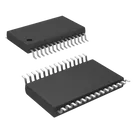
| Package | 30-pin TSSOP (DBT) |
| Pin count | 30 |
| Designator prefix | IC |
| Mount | Hardware |
| Datasheet | Datasheet |
| Pricing/availability | Mouser: $5.41, stock ~3.2K (as shown in project context) |
- The schematic currently represents all 30 pins as Terminal components (one per pin) such as AVDD, DVDD, IOVDD, DOUT, BCK, LRCK, etc.
- Datasheet URL
- A datasheet URL is already set on this part: Datasheet. No update needed.
- Datasheet scan and metadata extraction
- High SNR performance: PCM1861/63/65: 110 dB; PCM1860/62/64: 103 dB
- ADC sample rate: 8 kHz to 192 kHz
- Up to four independent ADC channels available
- Single-ended 2.1 VRMS FS input; differential 4.2 VRMS FS input
- Hardware control (PCM1860/61)
- Single 3.3 V power-supply operation
- Integrated high-performance audio PLL; master or slave audio interface
- Power: < 85 mW (PCM1860/61/62/63) at 3.3 V
Table
| Parameter | Min | Nom | Max | Unit | Notes |
|---|---|---|---|---|---|
| AVDD | 3.0 | 3.3 | 3.6 | V | Analog supply to AGND |
| DVDD | 3.0 | 3.3 | 3.6 | V | Digital supply to DGND |
| IOVDD (option 1) | 1.62 | 1.8 | 1.98 | V | 1.8 V I/O option |
| IOVDD (option 2) | 3.0 | 3.3 | 3.6 | V | 3.3 V I/O option |
| LDO pin voltage | IOVDD − 0.3 | IOVDD | IOVDD + 0.3 | V | LDO pin is input when bypassing with external 1.8 V |
| TA | −40 | — | 125 | °C | Operating ambient temperature |
Table
| Parameter | Condition | Min | Typ | Max | Unit |
|---|---|---|---|---|---|
| Full-scale input (SE) | 0 dB PGA | — | 2.1 | — | VRMS |
| Full-scale input (Diff) | 2.1 VRMS per pin | — | 4.2 | — | VRMS |
| SNR (SE) | 0 dB PGA, −60 dB input, master | — | 106 | — | dB |
| SNR (Diff) | 0 dB PGA, −60 dB input, master | — | 110 | — | dB |
| THD+N (Diff) | 0 dB PGA, −1 dB input, master | −93 | — | −85 | dB |
| THD+N (SE) | 0 dB PGA, −1 dB input, master | — | 87 | — | dB |
| PGA range | — | −12 | — | 32 | dB |
| Input impedance (per pin) | PCM1860/61/62/63 | — | 20 | — | kΩ |
| Energysense secondary ADC | Sampling rate | 8 | — | 192 | kHz |
Table
| Parameter | Typ |
|---|---|
| Mic bias voltage | 2.6 V |
| Mic bias current drive | 4 mA |
| Mic bias noise | 5 µVRMS |
Table
| Parameter | Condition | Min | Typ | Max |
|---|---|---|---|---|
| XTAL support | — | 15 | — | 35 MHz |
| MCLK frequency | 3.3 V on MCLK pin | 1 | — | 50 MHz |
| MCLK frequency | 1.8 V MCLK on XI pin | 1 | — | 50 MHz |
| MCLK duty cycle | 1.8 V MCLK | 48% | — | 52% |
| Max BCK | IOVDD = 3.3 V | — | — | 50 MHz |
| Max BCK | IOVDD = 1.8 V | — | — | 25 MHz |
Table
| Parameter | Value |
|---|---|
| ESD HBM | ±2000 V |
| ESD CDM | ±750 V |
| RθJA (DBT 30) | 79.6 °C/W |
| RθJC(top) | 15.1 °C/W |
| RθJB | 33.1 °C/W |
| ψJT | 0.4 °C/W |
| ψJB | 32.6 °C/W |
Table
| No. | Name | Type | Description |
|---|---|---|---|
| 1 | VINL2/VIN1M | Analog input | Analog input 2, L-channel (or differential M input for input 1) |
| 2 | VINR2/VIN2M | Analog input | Analog input 2, R-channel (or differential M input for input 2) |
| 3 | VINL1/VIN1P | Analog input | Analog input 1, L-channel (or differential P input for input 1) |
| 4 | VINR1/VIN2P | Analog input | Analog input 1, R-channel (or differential P input for input 2) |
| 5 | Mic Bias | Power | Microphone bias output |
| 6 | VREF | Power | Reference voltage output decoupling point (typically 0.5 AVDD). Connect 1 µF to AGND. |
| 7 | AGND | Power | Analog ground |
| 8 | AVDD | Power | Analog 3.3 V supply. Decouple 0.1 µF and 10 µF to AGND. |
| 9 | XO | Digital output | Crystal oscillator output |
| 10 | XI | Digital input | Crystal oscillator input or 1.8 V MCLK input |
| 11 | LDO | Power | Internal LDO decoupling output, or external 1.8 V input to bypass LDO. Decouple 0.1 µF and 10 µF to DGND. |
| 12 | DGND | Power | Digital ground |
| 13 | DVDD | Power | Digital 3.3 V supply. Decouple 0.1 µF and 10 µF to DGND. |
| 14 | IOVDD | Power | I/O supply (1.8 V or 3.3 V) |
| 15 | SCKI | Digital input | CMOS (3.3 V) master clock input |
| 16 | LRCK | Digital I/O | Audio word clock input/output |
| 17 | BCK | Digital I/O | Audio bit clock input/output |
| 18 | DOUT | Digital output | Audio data output |
| 19 | INT | Analog output | Interrupt for analog input detection (high = active, low = idle) |
| 20 | MD6 | Analog input | Analog MUX/gain select (with MD5, MD2); see table |
| 21 | MD5 | Analog input | Analog MUX/gain select |
| 22 | MD4 | Analog input | Audio format: high = left-justified, low = I2S |
| 23 | MD2 | Analog input | Analog MUX/gain select |
| 24 | MD3 | Digital input | Filter select: 0 = FIR, 1 = IIR low-latency |
| 25 | MD1 | Analog input | Audio interface mode (with MD0): 00 slave auto, 01 master 512×fS, 10 master 384×fS, 11 master 256×fS |
| 26 | MD0 | Analog input | Audio interface mode select (with MD1) |
| 27 | VINL4/VIN4M | Analog input | Analog input 4, L (or differential M for input 4) |
| 28 | VINR4/VIN3M | Analog input | Analog input 4, R (or differential M for input 3) |
| 29 | VINL3/VIN4P | Analog input | Analog input 3, L (or differential P for input 4) |
| 30 | VINR3/VIN3P | Analog input | Analog input 3, R (or differential P for input 3) |
- Package: DBT (TSSOP-30). Mechanical drawing: DBT0030A / R-PDSO-G30.
- Land pattern/dimensions should be taken from the linked package drawing. Numeric dimensions could not be machine-extracted here.
- Cross-check: symbol and footprint vs datasheet
- Pin count: 30 present in the symbol (30 Terminals). Matches the DBT package.
- Pin numbers and names match the datasheet mapping:
- VINL2/VIN1M is Pin 1 (matches datasheet).
- VINR3/VIN3P is Pin 30 (matches).
- SCKI is Pin 15; LRCK is Pin 16; BCK is Pin 17; DOUT is Pin 18 (all match).
- Supplies and grounds match numbering: AVDD=8, AGND=7, DVDD=13, DGND=12, IOVDD=14 (all match).
- Control pins MD0=26, MD1=25, MD2=23, MD3=24, MD4=22, MD5=21, MD6=20 (all match).
- Pin electrical types in the symbol are currently “Unspecified” for all pins. This won’t cause manufacturing errors, but it can reduce ERC effectiveness. Consider setting types to Power/Digital/Analog per the datasheet to improve checks.
- One footprint present with 30 pads named to match all pin names. Pad naming aligns with schematic pin names and datasheet names.
- Mismatch risks to verify before manufacturing:
- Land pattern/pitch/alignment: The project data does not expose pad pitch, body size, or pad geometry for automated verification here. Ensure the footprint matches DBT (TSSOP-30) per mechanical drawing, including:
- Correct lead pitch (TSSOP-30), lead span, pad length/width, and courtyard.
- Pin 1 indicator location consistent with symbol pin 1 (VINL2/VIN1M).
- Footprint rotation/origin matching your assembly data.
- Solder mask and paste apertures: verify they follow TI recommendations for DBT to avoid solder bridging or insufficient solder.
- Land pattern/pitch/alignment: The project data does not expose pad pitch, body size, or pad geometry for automated verification here. Ensure the footprint matches DBT (TSSOP-30) per mechanical drawing, including:
- If you’d like, I can help measure pad pitch and compare to the TI drawing once you confirm the intended land pattern values for DBT or provide a 2D footprint detail export.
- Absolute Maximum Ratings: the PDF section did not machine-extract during this pass. If you want, I can pull exact limits by querying a direct PDF URL for the datasheet (not the GPN page) and extract 7.1 explicitly.
Ready.
Reviews

- Wirelessly connects nets on schematic. Used to organize schematics and separate functional blocks. To wirelessly connect net portals, give them same designator. #portaljharwinbarrozo43.0M
- Wirelessly connects power nets on schematic. Identical to the net portal, but with a power symbol. Used to organize schematics and separate functional blocks. To wirelessly connect power net portals, give them the same designator. #portal #powerjharwinbarrozo11.4M
- A generic fixed resistor for rapid developing circuit topology. Save precious design time by seamlessly add more information to this part (value, footprint, etc.) as it becomes available. Standard resistor values: 1.0Ω 10Ω 100Ω 1.0kΩ 10kΩ 100kΩ 1.0MΩ 1.1Ω 11Ω 110Ω 1.1kΩ 11kΩ 110kΩ 1.1MΩ 1.2Ω 12Ω 120Ω 1.2kΩ 12kΩ 120kΩ 1.2MΩ 1.3Ω 13Ω 130Ω 1.3kΩ 13kΩ 130kΩ 1.3MΩ 1.5Ω 15Ω 150Ω 1.5kΩ 15kΩ 150kΩ 1.5MΩ 1.6Ω 16Ω 160Ω 1.6kΩ 16kΩ 160kΩ 1.6MΩ 1.8Ω 18Ω 180Ω 1.8KΩ 18kΩ 180kΩ 1.8MΩ 2.0Ω 20Ω 200Ω 2.0kΩ 20kΩ 200kΩ 2.0MΩ 2.2Ω 22Ω 220Ω 2.2kΩ 22kΩ 220kΩ 2.2MΩ 2.4Ω 24Ω 240Ω 2.4kΩ 24kΩ 240kΩ 2.4MΩ 2.7Ω 27Ω 270Ω 2.7kΩ 27kΩ 270kΩ 2.7MΩ 3.0Ω 30Ω 300Ω 3.0KΩ 30KΩ 300KΩ 3.0MΩ 3.3Ω 33Ω 330Ω 3.3kΩ 33kΩ 330kΩ 3.3MΩ 3.6Ω 36Ω 360Ω 3.6kΩ 36kΩ 360kΩ 3.6MΩ 3.9Ω 39Ω 390Ω 3.9kΩ 39kΩ 390kΩ 3.9MΩ 4.3Ω 43Ω 430Ω 4.3kΩ 43KΩ 430KΩ 4.3MΩ 4.7Ω 47Ω 470Ω 4.7kΩ 47kΩ 470kΩ 4.7MΩ 5.1Ω 51Ω 510Ω 5.1kΩ 51kΩ 510kΩ 5.1MΩ 5.6Ω 56Ω 560Ω 5.6kΩ 56kΩ 560kΩ 5.6MΩ 6.2Ω 62Ω 620Ω 6.2kΩ 62KΩ 620KΩ 6.2MΩ 6.8Ω 68Ω 680Ω 6.8kΩ 68kΩ 680kΩ 6.8MΩ 7.5Ω 75Ω 750Ω 7.5kΩ 75kΩ 750kΩ 7.5MΩ 8.2Ω 82Ω 820Ω 8.2kΩ 82kΩ 820kΩ 8.2MΩ 9.1Ω 91Ω 910Ω 9.1kΩ 91kΩ 910kΩ 9.1MΩ #generics #CommonPartsLibraryjharwinbarrozo1.5M
- A generic fixed capacitor ideal for rapid circuit topology development. You can choose between polarized and non-polarized types, its symbol and the footprint will automatically adapt based on your selection. Supported options include standard SMD sizes for ceramic capacitors (e.g., 0402, 0603, 0805), SMD sizes for aluminum electrolytic capacitors, and through-hole footprints for polarized capacitors. Save precious design time by seamlessly add more information to this part (value, footprint, etc.) as it becomes available. Standard capacitor values: 1.0pF 10pF 100pF 1000pF 0.01uF 0.1uF 1.0uF 10uF 100uF 1000uF 10,000uF 1.1pF 11pF 110pF 1100pF 1.2pF 12pF 120pF 1200pF 1.3pF 13pF 130pF 1300pF 1.5pF 15pF 150pF 1500pF 0.015uF 0.15uF 1.5uF 15uF 150uF 1500uF 1.6pF 16pF 160pF 1600pF 1.8pF 18pF 180pF 1800pF 2.0pF 20pF 200pF 2000pF 2.2pF 22pF 20pF 2200pF 0.022uF 0.22uF 2.2uF 22uF 220uF 2200uF 2.4pF 24pF 240pF 2400pF 2.7pF 27pF 270pF 2700pF 3.0pF 30pF 300pF 3000pF 3.3pF 33pF 330pF 3300pF 0.033uF 0.33uF 3.3uF 33uF 330uF 3300uF 3.6pF 36pF 360pF 3600pF 3.9pF 39pF 390pF 3900pF 4.3pF 43pF 430pF 4300pF 4.7pF 47pF 470pF 4700pF 0.047uF 0.47uF 4.7uF 47uF 470uF 4700uF 5.1pF 51pF 510pF 5100pF 5.6pF 56pF 560pF 5600pF 6.2pF 62pF 620pF 6200pF 6.8pF 68pF 680pF 6800pF 0.068uF 0.68uF 6.8uF 68uF 680uF 6800uF 7.5pF 75pF 750pF 7500pF 8.2pF 82pF 820pF 8200pF 9.1pF 91pF 910pF 9100pF #generics #CommonPartsLibraryjharwinbarrozo1.5M
- A generic fixed inductor for rapid developing circuit topology. *You can now change the footprint and 3D model at the top level anytime you want. This is the power of #genericsjharwinbarrozo15.6k
- An electrical connector acting as reusable interface to a conductor and creating a point where external circuits can be connected.Terminal
- 47 kOhms ±5% 0.125W, 1/8W Chip Resistor 0805 (2012 Metric) Automotive AEC-Q200 Thick Film #forLedBlinkjharwinbarrozo1.2M
- 10uF Capacitor Aluminum Polymer 20% 16V SMD 5x5.3mm #forLedBlink #commonpartslibrary #capacitor #aluminumpolymer #radialcanjharwinbarrozo1.2M
- Yellow 595nm LED Indication - Discrete 1.7V 1206 (3216 Metric) #forLedBlinkjharwinbarrozo1.1M


Pricing & Availability
See prices from popular manufacturers for your project.
Assets

PCM1861DBT-thumb.png
PCM1861DBT-thumbThumbnailPCM1861DBT
SOP50P640X120-30N.kicad_modFootprintPCM1861DBT
PCM1861DBT.stp3D Model
PCM1861DBT
PCM1861DBT Symbol.svgDefaultControls
Welcome 👋
Flux accelerates your PCB design with AI.
Create your account to start using this component and bring your ideas to life.