Part Information Review and Datasheet Update
2:26
Evaluating project parameters.
Assessing update actions.
Checking if I can make the changes for you.
Reviewing the bill of materials.
Analyzing the schematic.
Running multiple web searches.
Found 10 results.
Found 10 results.
Looking for "part description and overview" in HSWA4-63DR+.pdf
Looking for "package information mechanical dimensions package case and exposed pad" in HSWA4-63DR+.pdf
Looking for "pin connection table or pin description" in HSWA4-63DR+.pdf
Looking for "absolute maximum ratings and supply voltage" in HSWA4-63DR+.pdf
Looking for "operating frequency insertion loss isolation control voltage current temperature" in HSWA4-63DR+.pdf
Analyzing the PCB layout.
Looking for "exposed paddle pad 25 ground description" in HSWA4-63DR+.pdf
Looking for "package drawing pad 25 exposed paddle" in HSWA4-63DR+.pdf
Looking for "control truth table control 1 control 2 control 3 routing" in HSWA4-63DR+.pdf
Confirming pin count.
Reviewing the bill of materials.
Part review summary
| Field | Result |
|---|---|
| MPN | HSWA4-63DR+ |
| Manufacturer | Mini-Circuits |
| Description | MMIC absorptive SP4T RF switch with internal driver |
| Frequency range | 30 MHz to 6000 MHz |
| Supply voltage | 2.3 V to 5.5 V |
| Absolute max VDD | -0.3 V to +5.5 V |
| Operating temperature | -40 C to +105 C |
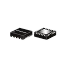
| Package | DG984-1, 4 mm x 4 mm |
| Lead style | 24-lead QFN / MCLP with exposed paddle |
| Pad count including EP | 25 pads total |
| Typical insertion loss | 0.9 dB to 1.8 dB over band |
| Typical isolation | 61 dB down to 30 dB over band |
What matches
| Area | Status | Notes |
|---|---|---|
| Footprint package family | Good | The footprint is a 4 mm x 4 mm 24-lead package with exposed pad, consistent with the datasheet. |
| Exposed paddle | Good | Pad 25 is present and the datasheet says the exposed paddle is ground. |
| Total terminal count | Good | Project has 25 terminals, which matches 24 leads + exposed paddle. |
| Control/VDD terminal names present | Good | CONTROL1, CONTROL2, CONTROL3, and VDD exist. |
Pin mapping mismatches
Datasheet pinout reference
| Pad | Function |
|---|---|
| 1 | RF4 |
| 2 | GND |
| 3 | RF3 |
| 4 | GND |
| 5 | RF2 |
| 6 | GND |
| 7 | RF1 |
| 8 | GND |
| 9 | RF COM |
| 10-18 | GND |
| 19 | Control 3 |
| 20 | VDD |
| 21 | Control 2 |
| 22 | Control 1 |
| 23-24 | GND |
| 25 | Exposed paddle, GND |
- The official datasheet URL is available.
- The footprint package style appears correct.
- The symbol terminal numbering is substantially incorrect versus the datasheet.
- Because of that, the current part would connect several RF, control, and supply pins to the wrong footprint pads.


Welcome 👋
Flux accelerates your PCB design with AI.
Create your account to start using this component and bring your ideas to life.