Part Datasheet and Footprint Verification
3:54
Analy.
Processing.
Understanding.
Navig.
Cross.
Using Schematic Tool.
Using PCB Layout Tool.
Looking for "Absolute Maximum Ratings table" in esp32-s3_datasheet_en.pdf
Looking for "Recommended Operating Conditions" in esp32-s3_datasheet_en.pdf
Looking for "Electrical Characteristics" in esp32-s3_datasheet_en.pdf
Looking for "Current consumption" in esp32-s3_datasheet_en.pdf
Looking for "Power supply voltage" in esp32-s3_datasheet_en.pdf
Looking for "GPIO voltage levels thresholds VIH VIL VOH VOL" in esp32-s3_datasheet_en.pdf
Looking for "Wi-Fi features" in esp32-s3_datasheet_en.pdf
Looking for "Bluetooth Low Energy features" in esp32-s3_datasheet_en.pdf
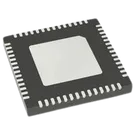
Looking for "Package information mechanical dimensions" in esp32-s3_datasheet_en.pdf
Looking for "Package dimensions QFN" in esp32-s3_datasheet_en.pdf
Looking for "Pin description table" in esp32-s3_datasheet_en.pdf
Looking for "Pin definitions list of pins and functions" in esp32-s3_datasheet_en.pdf
Looking for "Pin count for ESP32-S3 packages" in esp32-s3_datasheet_en.pdf
Looking for "Naming ESP32-S3R16V variant meaning and embedded memory" in esp32-s3_datasheet_en.pdf
Looking for "SPI interface pins SPIQ SPID SPICLK SPIWP SPIHD VDD_SPI" in esp32-s3_datasheet_en.pdf
Looking for "Strapping pins list and default states" in esp32-s3_datasheet_en.pdf
Looking for "External crystal pins XTAL_P XTAL_N and 32K XTAL_32K_P XTAL_32K_N requirements" in esp32-s3_datasheet_en.pdf
Looking for "RF input LNA_IN pin and matching network guidelines" in esp32-s3_datasheet_en.pdf
Looking for "Thermal pad exposed pad connection recommendation" in esp32-s3_datasheet_en.pdf
Using PCB Layout Tool.
- Review of available part information in the project
- MPN: ESP32-S3R16V
- Manufacturer: Espressif
- Part type: Integrated Circuits
- Designator prefix: IC
- Datasheet property: Present — Datasheet
- Package: Not explicitly set in properties (symbol and footprint exist)
- Symbol pins present: 57 total (numbered 1..57), including LNA_IN (Pin 1), dual VDD3P3_1/VDD3P3_2 (Pins 2/3), CHIP_PU (Pin 4), and GND (Pin 57).
- Footprint: Present with pad names matching symbol pins (pads include LNA_IN, GPIOx, SPIx, VDDA_1/2, GND, etc.)
- Datasheet URL check and update
- Datasheet already set: Datasheet
- No change required.
- Datasheet scan — extracted metadata
Table
| Parameter | Description | Min | Max | Unit |
|---|---|---|---|---|
| Input power pins | Allowed input voltage | –0.3 | 3.6 | V |
| Ioutput | Cumulative IO output current | — | 1500 | mA |
| TSTORE | Storage temperature | –40 | 150 | °C |
Table
| Parameter | Description | Min | Typ | Max | Unit | Notes |
|---|---|---|---|---|---|---|
| VDDA, VDD3P3 | Recommended input voltage | 3.0 | 3.3 | 3.6 | V | 1 |
| VDD3P3_RTC | Recommended input voltage | 3.0 | 3.3 | 3.6 | V | 2 |
| VDD_SPI (as input) | — | — | 1.8 / 3.3 | 3.6 | V | 2 |
| VDD3P3_CPU | Recommended input voltage | 3.0 | 3.3 | 3.6 | V | 3 |
| IVDD | Cumulative input current | 0.5 | — | — | A | 4 |
Table
| Parameter | Description | Typ | Unit | Notes |
|---|---|---|---|---|
| RSPI | VDD_SPI powered by VDD3P3_RTC via RSPI for 3.3 V flash/PSRAM | 14 | Ω | 2 |
| ISPI | Output current when VDD_SPI powered by 1.8 V Flash Voltage Regulator | 40 | mA | — |
Table
| Parameter | Description | Min | Typ | Max | Unit |
|---|---|---|---|---|---|
| CIN | Pin capacitance | — | 2 | — | pF |
| VIH | High-level input voltage | 0.75 × VDD | — | VDD + 0.3 | V |
| VIL | Low-level input voltage | –0.3 | — | 0.25 × VDD | V |
| VIL_nRST | CHIP_PU reset voltage | –0.3 | — | 0.25 × VDD | V |
Table
| Parameter | Description | Min | Max | Unit |
|---|---|---|---|---|
| DNL | Differential nonlinearity | –4 | 4 | LSB |
| INL | Integral nonlinearity | –8 | 8 | LSB |
| Sampling rate | — | — | 100 kSPS | — |
Table
| Mode | Condition | Value |
|---|---|---|
| Wi‑Fi TX | 802.11b, 1 Mbps, @21 dBm | 340 mA (peak) |
| Wi‑Fi TX | 802.11g, 54 Mbps, @19 dBm | 291 mA (peak) |
| Wi‑Fi TX | 802.11n, HT20, MCS7, @18.5 dBm | 283 mA (peak) |
| Wi‑Fi TX | 802.11n, HT40, MCS7, @18 dBm | 286 mA (peak) |
| Wi‑Fi RX | 802.11b/g/n, HT20 | 88 mA (peak) |
| Wi‑Fi RX | 802.11n, HT40 | 91 mA (peak) |
| BLE TX | @ 21.0 dBm | 335 mA (peak) |
| BLE TX | @ 9.0 dBm | 193 mA (peak) |
| BLE TX | @ 0 dBm | 176 mA (peak) |
| BLE TX | @ –15.0 dBm | 116 mA (peak) |
| BLE RX | — | 93 mA (peak) |
| Light‑sleep | VDD_SPI/Wi‑Fi off, GPIOs Hi‑Z | 240 µA (typ) |
| Deep‑sleep | RTC mem + peripherals on | 8 µA (typ) |
| Deep‑sleep | RTC mem on, peripherals off | 7 µA (typ) |
| Power off | CHIP_PU low | 1 µA (typ) |
Table
| Range | Notable pins in range |
|---|---|
| 1–4 | LNA_IN(1), VDD3P3(2,3), CHIP_PU(4) |
| 5–18 | GPIO0..GPIO13 |
| 19–27 | GPIO14, VDD3P3_RTC(20), XTAL_32K_P/N(21/22), GPIO17..GPIO21 |
| 28–37 | SPICS1(28), VDD_SPI(29), SPIHD/WP/CS0/CLK/Q/D(30–35), SPICLK_N/P(36/37) |
| 38–46 | GPIO33..GPIO38, MTCK(44), MTDO(45), VDD3P3_CPU(46) |
| 47–52 | MTDI(47), MTMS(48), U0TXD(49), U0RXD(50), GPIO45(51), GPIO46(52) |
| 53–57 | XTAL_N(53), XTAL_P(54), VDDA(55,56), GND(57, exposed pad) |
Table
| Pin | Default |
|---|---|
| GPIO0 | Weak pull‑up (1) |
| GPIO3 | Floating |
| GPIO45 | Weak pull‑down (0) |
| GPIO46 | Weak pull‑down (0) |
Table
| Part | In‑package Flash | In‑package PSRAM | Ambient temp | VDD_SPI | Chip rev |
|---|---|---|---|---|---|
| ESP32‑S3R16V | — | 16 MB (Octal SPI) | –40 ∼ 65 °C | 1.8 V | v0.2 |
- Wi‑Fi: 802.11b/g/n; HT20/HT40; MCS0‑7; data rate up to 150 Mbps; RX STBC; adjustable TX power; antenna diversity with external RF switch.
- Bluetooth LE: Bluetooth 5 + Mesh; PHYs: 1M, 2M, Coded (125/500 kbps); Class 1 TX power; LE Advertising Extensions; multiple sets; simultaneous advertising and scanning.
- Package: QFN56 (7×7 mm), exposed ground pad present (datasheet Figure 7‑1).
- Thermal pad guidance: connect EPAD to ground with at least nine ground vias; use paste windowing as recommended.
- 50 Ω controlled‑impedance RF trace, CLC matching near the chip; use 0201 parts; stub on first capacitor to suppress harmonics; include antenna ESD.
- Main crystal: 40 MHz only; include ~24 nH series element on XTAL_P initially; tune C1/C4 per CL formula.
- 32.768 kHz RTC crystal optional; ESR ≤ 70 kΩ; bias resistor 5 MΩ < R ≤ 10 MΩ if needed.
- Cross‑check: symbol and footprint vs datasheet
- Pin count: Symbol contains 57 pins (1..57) including the exposed pad GND as Pin 57 — matches QFN56 + EPAD in the datasheet.
- Naming and numbering: Spot‑checks align with Table 2‑1 — e.g., LNA_IN = Pin 1, VDD3P3_1 = Pin 2, CHIP_PU = Pin 4, VDD_SPI = Pin 29, SPI bus pins (30–35), SPICLK_N/P (36/37), VDD3P3_CPU = Pin 46, U0TXD/U0RXD = Pins 49/50, VDDA_1/VDDA_2 = Pins 55/56, GND = Pin 57.
- Result: No symbol mismatches found.
- Pad coverage: Footprint includes pads named for all symbol pins, including an EPAD labeled GND — consistent with datasheet requirement for an exposed ground pad.
- Mechanical dimensions: The footprint data exposed to the tool does not include pad pitch/size or body size; thus, I cannot verify QFN56 7×7 mm outline, pin‑1 orientation marker, or pad pitch against the datasheet drawing.
- Thermal viaing: Datasheet calls for “at least nine” ground vias in the EPAD; via stitching cannot be verified from the available footprint metadata.
- Missing/uncertain: Package properties are not explicitly set in the part metadata; consider setting “QFN56, 7×7 mm” to avoid ordering ambiguity.
- Verification needed: Manually confirm in the Footprint editor that:
- Body size is 7×7 mm and matches the ESP32‑S3 QFN56 land pattern.
- Pin pitch and pad dimensions match the datasheet’s QFN56 drawing.
- Pin‑1 marker and pad numbering around the perimeter follow the datasheet orientation.
- EPAD solder paste windowing and via‑in‑pad/thermal vias follow the recommendations (≥ 9 vias tied to GND).
- Electrical variant note: For ESP32‑S3R16V, VDD_SPI domain is 1.8 V (per Table 1‑1). Ensure any reference designs and net annotations reflect 1.8 V for in‑package PSRAM/flash operation.
Ready.
Reviews

- Wirelessly connects nets on schematic. Used to organize schematics and separate functional blocks. To wirelessly connect net portals, give them same designator. #portaljharwinbarrozo43.0M
- Wirelessly connects power nets on schematic. Identical to the net portal, but with a power symbol. Used to organize schematics and separate functional blocks. To wirelessly connect power net portals, give them the same designator. #portal #powerjharwinbarrozo11.4M
- A generic fixed resistor for rapid developing circuit topology. Save precious design time by seamlessly add more information to this part (value, footprint, etc.) as it becomes available. Standard resistor values: 1.0Ω 10Ω 100Ω 1.0kΩ 10kΩ 100kΩ 1.0MΩ 1.1Ω 11Ω 110Ω 1.1kΩ 11kΩ 110kΩ 1.1MΩ 1.2Ω 12Ω 120Ω 1.2kΩ 12kΩ 120kΩ 1.2MΩ 1.3Ω 13Ω 130Ω 1.3kΩ 13kΩ 130kΩ 1.3MΩ 1.5Ω 15Ω 150Ω 1.5kΩ 15kΩ 150kΩ 1.5MΩ 1.6Ω 16Ω 160Ω 1.6kΩ 16kΩ 160kΩ 1.6MΩ 1.8Ω 18Ω 180Ω 1.8KΩ 18kΩ 180kΩ 1.8MΩ 2.0Ω 20Ω 200Ω 2.0kΩ 20kΩ 200kΩ 2.0MΩ 2.2Ω 22Ω 220Ω 2.2kΩ 22kΩ 220kΩ 2.2MΩ 2.4Ω 24Ω 240Ω 2.4kΩ 24kΩ 240kΩ 2.4MΩ 2.7Ω 27Ω 270Ω 2.7kΩ 27kΩ 270kΩ 2.7MΩ 3.0Ω 30Ω 300Ω 3.0KΩ 30KΩ 300KΩ 3.0MΩ 3.3Ω 33Ω 330Ω 3.3kΩ 33kΩ 330kΩ 3.3MΩ 3.6Ω 36Ω 360Ω 3.6kΩ 36kΩ 360kΩ 3.6MΩ 3.9Ω 39Ω 390Ω 3.9kΩ 39kΩ 390kΩ 3.9MΩ 4.3Ω 43Ω 430Ω 4.3kΩ 43KΩ 430KΩ 4.3MΩ 4.7Ω 47Ω 470Ω 4.7kΩ 47kΩ 470kΩ 4.7MΩ 5.1Ω 51Ω 510Ω 5.1kΩ 51kΩ 510kΩ 5.1MΩ 5.6Ω 56Ω 560Ω 5.6kΩ 56kΩ 560kΩ 5.6MΩ 6.2Ω 62Ω 620Ω 6.2kΩ 62KΩ 620KΩ 6.2MΩ 6.8Ω 68Ω 680Ω 6.8kΩ 68kΩ 680kΩ 6.8MΩ 7.5Ω 75Ω 750Ω 7.5kΩ 75kΩ 750kΩ 7.5MΩ 8.2Ω 82Ω 820Ω 8.2kΩ 82kΩ 820kΩ 8.2MΩ 9.1Ω 91Ω 910Ω 9.1kΩ 91kΩ 910kΩ 9.1MΩ #generics #CommonPartsLibraryjharwinbarrozo1.5M
- A generic fixed capacitor ideal for rapid circuit topology development. You can choose between polarized and non-polarized types, its symbol and the footprint will automatically adapt based on your selection. Supported options include standard SMD sizes for ceramic capacitors (e.g., 0402, 0603, 0805), SMD sizes for aluminum electrolytic capacitors, and through-hole footprints for polarized capacitors. Save precious design time by seamlessly add more information to this part (value, footprint, etc.) as it becomes available. Standard capacitor values: 1.0pF 10pF 100pF 1000pF 0.01uF 0.1uF 1.0uF 10uF 100uF 1000uF 10,000uF 1.1pF 11pF 110pF 1100pF 1.2pF 12pF 120pF 1200pF 1.3pF 13pF 130pF 1300pF 1.5pF 15pF 150pF 1500pF 0.015uF 0.15uF 1.5uF 15uF 150uF 1500uF 1.6pF 16pF 160pF 1600pF 1.8pF 18pF 180pF 1800pF 2.0pF 20pF 200pF 2000pF 2.2pF 22pF 20pF 2200pF 0.022uF 0.22uF 2.2uF 22uF 220uF 2200uF 2.4pF 24pF 240pF 2400pF 2.7pF 27pF 270pF 2700pF 3.0pF 30pF 300pF 3000pF 3.3pF 33pF 330pF 3300pF 0.033uF 0.33uF 3.3uF 33uF 330uF 3300uF 3.6pF 36pF 360pF 3600pF 3.9pF 39pF 390pF 3900pF 4.3pF 43pF 430pF 4300pF 4.7pF 47pF 470pF 4700pF 0.047uF 0.47uF 4.7uF 47uF 470uF 4700uF 5.1pF 51pF 510pF 5100pF 5.6pF 56pF 560pF 5600pF 6.2pF 62pF 620pF 6200pF 6.8pF 68pF 680pF 6800pF 0.068uF 0.68uF 6.8uF 68uF 680uF 6800uF 7.5pF 75pF 750pF 7500pF 8.2pF 82pF 820pF 8200pF 9.1pF 91pF 910pF 9100pF #generics #CommonPartsLibraryjharwinbarrozo1.5M
- A generic fixed inductor for rapid developing circuit topology. *You can now change the footprint and 3D model at the top level anytime you want. This is the power of #genericsjharwinbarrozo15.6k
- An electrical connector acting as reusable interface to a conductor and creating a point where external circuits can be connected.Terminal
- 47 kOhms ±5% 0.125W, 1/8W Chip Resistor 0805 (2012 Metric) Automotive AEC-Q200 Thick Film #forLedBlinkjharwinbarrozo1.2M
- 10uF Capacitor Aluminum Polymer 20% 16V SMD 5x5.3mm #forLedBlink #commonpartslibrary #capacitor #aluminumpolymer #radialcanjharwinbarrozo1.2M
- Yellow 595nm LED Indication - Discrete 1.7V 1206 (3216 Metric) #forLedBlinkjharwinbarrozo1.1M


Pricing & Availability
See prices from popular manufacturers for your project.
Assets

ESP32-S3R16V-thumb.png
ESP32-S3R16V-thumbThumbnail
ESP32-S3R16V
ESP32-S3R16V Symbol.svgDefaultESP32-S3R16V
ESP32-S3R16V.stp3D ModelESP32-S3R16V
QFN40P700X700X90-57N-D.kicad_modFootprintControls
Welcome 👋
Flux accelerates your PCB design with AI.
Create your account to start using this component and bring your ideas to life.