Part Review and Datasheet Update
Thought for 3 mins 20 sec
I completed the review. Since this part project already has a datasheet-related URL set in its properties, I did not modify the part properties in step 2.
1) Available part information in the project
Table
| Field | Value |
|---|---|
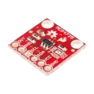
| Project / Part | BOB-12918 |
| Description | MCP4725 DAC BREAKOUT |
| Manufacturer | SparkFun |
| MPN | BOB-12918 |
| Datasheet URL property | https://www.sparkfun.com/products/12918 |
| Schematic contents | Terminal-only breakout symbol with 8 terminals |
| Footprint asset | BOB12918.kicad_mod |
| Breakout electrical pins | SCL, SDA, VCC, GND_1, OUT, GND_2 |
| Mechanical pins | MH1, MH2 |
| Nets in schematic | None defined yet |
Table
| Item | Status |
|---|---|
| Existing project datasheet-related URL | Present |
| URL type | SparkFun product page, not a direct PDF datasheet |
| Additional references found | SparkFun breakout PDF and official MCP4725 silicon datasheet |
Table
| Category | Summary |
|---|---|
| Breakout function | SparkFun breakout for MCP4725, a single-channel 12-bit I2C DAC with EEPROM |
| Board-level extras | I2C pull-ups, address jumper, decoupling capacitor, dual GND breakout, two mounting holes |
| Interface | I2C: 100 kbps, 400 kbps, 3.4 Mbps |
| Supply range | 2.7 V to 5.5 V |
| Output | Rail-to-rail buffered analog output |
| EEPROM | Nonvolatile DAC setting retention through power-off |
| Typical settling time | 6 µs |
Table
| Parameter | Rating |
|---|---|
| VDD | 6.5 V |
| All inputs/outputs w.r.t. VSS | -0.3 V to VDD + 0.3 V |
| Current at input pins | ±2 mA |
| Current at supply pins | ±50 mA |
| Current at output pins | ±25 mA |
| Storage temperature | -65°C to +150°C |
| Ambient temperature with power applied | -55°C to +125°C |
| Maximum junction temperature | +150°C |
| ESD | >= 6 kV HBM, >= 400 V MM |
Table
Table
| Parameter | Value |
|---|---|
| Resolution | 12 bits |
| Supply current | 210 µA typ, 400 µA max |
| Power-down current | 0.06 µA typ, 2.0 µA max |
| INL | ±2 LSB typ, ±14.5 LSB max |
| DNL | ±0.2 LSB typ, ±0.75 LSB max |
| Offset error | 0.75% FSR typ |
| Gain error | -0.1% FSR typ, ±2% FSR max |
| Reference | Uses VDD as reference |
| Settling time | 6 µs typ |
Table
Table
| IC pin name | Function |
|---|---|
| VOUT | Analog output |
| VDD | Supply and DAC reference input |
| VSS | Ground |
| SDA | Open-drain I2C data, requires pull-up |
| SCL | Open-drain I2C clock, requires pull-up |
| A0 | I2C address select |
Table
| Feature | Detail |
|---|---|
| I2C pull-ups | Two 4.7k Resistor pull-ups on SDA and SCL |
| Decoupling | One 0.1uF Capacitor |
| Address selection | 10k Resistor and solder jumper; default address 0x60, alternate 0x61 |
| Grounds | Two breakout ground pins are intentionally provided |
Table
| Item | Dimension / Detail |
|---|---|
| IC package option | 6-lead SOT-23 or DFN option in silicon datasheet |
| IC package drawing data | Exact SOT-23 mechanical drawing was not returned from the scanned Microchip PDF pages |
| Part-project footprint outline | 15.24 mm x 15.24 mm from the footprint asset |
| Header pad pitch | 2.54 mm |
| Header drill | 1.11 mm |
| Header pad size | 1.665 mm |
| Mount hole drill | 2.0 mm |
| Mount hole pad size | 3.0 mm |
| Mount-hole center spacing | 11.43 mm vertical |
Table
| Check | Result | Notes |
|---|---|---|
| Pin count vs breakout | Pass | Project has 6 electrical breakout pins plus 2 mounting holes |
| Pin numbering | Pass | Project numbering 1..6 matches SparkFun breakout header mapping |
| Pin naming | Pass | SCL, SDA, VCC, GND_1, OUT, GND_2 align with the breakout schematic |
| Dual GND pins | Pass | SparkFun schematic shows two separate ground breakout pins; project reflects that |
| Mounting holes | Pass | Two mechanical holes exist in both symbol and footprint |
| Footprint geometry | Pass | Footprint dimensions and hole spacing are internally consistent with a small breakout board |
| Risk of board-ordering confusion | Warning | Project description/MPN clearly describe the breakout, but the datasheet property points to the product page rather than a direct PDF |
| Risk of bare-IC ordering confusion | Warning | The part project represents the breakout board, not the bare MCP4725 IC; users could confuse these if they look only at the silicon datasheet |
| Risk of manufacturing failure from pin mismatch | No mismatch found | I did not find a header pin-order or mounting-hole mismatch |
| Risk of schematic misuse | Minor warning | No nets are defined yet in the part project, so functional validation of connectivity is not possible from the current schematic alone |
Table
| Severity | Finding | Why it matters |
|---|---|---|
| Medium | Datasheet property is a product page, not a direct datasheet PDF | Makes downstream review and part verification less reliable |
| Medium | Metadata is incomplete for package typing | The project does not explicitly state that this is a breakout module footprint, not a bare IC package |
| Low | Pin terminal types are all Unspecified | Not a manufacturing blocker, but it weakens ERC clarity if reused in larger designs |
Table
| Verdict | Outcome |
|---|---|
| Symbol-to-breakout pin mapping | Looks correct |
| Footprint-to-breakout intent | Looks correct |
| Manufacturing-critical mismatch found | No |
| Metadata cleanup recommended | Yes |
If you want, I can next check whether I’m allowed to update the part metadata so the datasheet points directly to the PDF and the package/part description more clearly indicate that this is a SparkFun breakout board module rather than the bare MCP4725 IC.
Fix datasheet property
Check review issues
Inspect footprint details