Part Datasheet Review and Verification
7:03
Processing.
Using Schematic Tool.
Using PCB Layout Tool.
Using BOM Tool.
Looking for "part overview including package, pin count, description, ordering or product summary" in _20181120__APA_102-2020-256-8.pdf
Looking for "absolute maximum ratings" in _20181120__APA_102-2020-256-8.pdf
Looking for "recommended operating conditions" in _20181120__APA_102-2020-256-8.pdf
Looking for "electrical characteristics" in _20181120__APA_102-2020-256-8.pdf
Looking for "pin descriptions or pin assignment" in _20181120__APA_102-2020-256-8.pdf
Looking for "package dimensions mechanical drawing" in _20181120__APA_102-2020-256-8.pdf
Looking for "features special features applications" in _20181120__APA_102-2020-256-8.pdf
Running multiple web searches.
Found 1 results.
Found 1 results.
Looking for "pin assignment pin descriptions" in 3587.html
Looking for "package dimensions mechanical drawing" in 3587.html
Looking for "electrical characteristics" in 3587.html
Looking for "absolute maximum ratings" in APA102_2020_8A_LED_Datasheet-3574735.pdf
Looking for "recommended operating conditions" in APA102_2020_8A_LED_Datasheet-3574735.pdf
Looking for "electrical characteristics" in APA102_2020_8A_LED_Datasheet-3574735.pdf
Looking for "pin assignment pin descriptions" in APA102_2020_8A_LED_Datasheet-3574735.pdf
Looking for "package dimensions mechanical drawing" in APA102_2020_8A_LED_Datasheet-3574735.pdf
Looking for "features special features product summary" in APA102_2020_8A_LED_Datasheet-3574735.pdf
Looking for "pin 7 function description" in APA102_2020_8A_LED_Datasheet-3574735.pdf
Looking for "pin 8 function description" in APA102_2020_8A_LED_Datasheet-3574735.pdf
Looking for "No. 7 Symbol Function description" in APA102_2020_8A_LED_Datasheet-3574735.pdf
Looking for "No. 8 Symbol Function description" in APA102_2020_8A_LED_Datasheet-3574735.pdf
Looking for "full pin table including pins 7 and 8" in APA102_2020_8A_LED_Datasheet-3574735.pdf
Organ.
Ident.
Part metadata
| Field | Value |
|---|---|
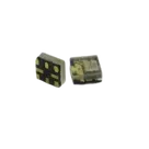
| Part | APA102-2020 |
| Description | RGB LED with integrated control IC, two-wire clock/data interface, cascaded pixel device |
| MPN | APA102-2020 |
| Package | 2020 SMD, 2.0 mm x 2.0 mm x 0.75 mm in the PDF summary |
| Variant noted in datasheet | APA-102-2020-256-8A |
| Pin count | 8 pins |
| Datasheet | |
| Key project properties | Manufacturer: Shenzhen LED Color Opto Electronic CO., LTD.; Designator Prefix: LED |
Extracted feature summary
| Category | Extracted data |
|---|---|
| Interface | Two-wire serial interface: DATA and CLK |
| Dimming | 256 grayscale levels, plus 32-level global brightness adjustment |
| Output type | Integrated RGB LED + driver IC |
| PWM | 20 kHz PWM frequency |
| Cascade support | Yes, with clock and data forwarding |
| Supply | 5.0 V to 5.5 V operating supply from extracted electrical table |
| LED current | Max LED output current listed as 18 mA in max ratings |
| Viewing angle | 120 deg |
| Manufacturing notes | RoHS, compatible with automatic placement and IR reflow, JEDEC level 3 preconditioning |
Absolute maximum ratings
| Parameter | Value |
|---|---|
| IC power supply voltage | -0.4 V to +5.5 V |
| Logic input voltage | -0.4 V to VDD + 0.4 V |
| Data signal rate | 15 MHz |
| ESD | 2000 V |
| Max LED output current | 18 mA |
| Soldering temperature | 260 C |
| Operating temperature range | -40 C to +85 C |
| Storage temperature range | -40 C to +105 C |
Recommended operating conditions / electrical characteristics
| Parameter | Min | Typ | Max | Unit |
|---|---|---|---|---|
| Supply voltage VDD | 5.0 | 5.5 | V | |
| Data signal rate FCLK | 5 | MHz | ||
| Input high voltage VIH | 0.7 x VDD | V | ||
| Input low voltage VIL | 0.3 x VDD | V | ||
| Clock high width TCLKH | 30 | ns | ||
| Clock low width TCLKL | 30 | ns | ||
| Data setup time TSETUP | 10 | ns | ||
| Data hold time THOLD | 5 | ns | ||
| PWM frequency FPWM | 20 | kHz | ||
| Static power consumption IDD | 0.7 | mA |
Table
Package / mechanical data
| Item | Value |
|---|---|
| Body size | 2.00 mm x 2.00 mm |
| Height | 0.75 mm from PDF mirror |
| Tolerance | +-0.1 mm unless otherwise specified |
| Recommended pad layout | Present in datasheet |
| Reflow compatibility | Yes |
Cross-check result
| Check | Result | Notes |
|---|---|---|
| Pin count | Pass | Project has 8 symbol pins and PCB pads |
| Pin naming | Pass | CO, CI, DO, DI, VDD_1, VDD_2, GND_1, GND_2 align with the 8-pin package concept |
| Pin numbering | Pass | Symbol numbering maps cleanly to the extracted function list |
| Functional directionality | Mostly pass | Clock/data input and output roles are represented correctly |
| Footprint pad count | Pass | PCB footprint exposes 8 pads matching the symbol |
| Footprint land pattern dimensions | Needs manual verification | Current PCB inspection exposed pad identities but not enough geometry detail to prove the land pattern matches the datasheet's recommended pad dimensions |
Issues / risks flagged
| Severity | Issue | Why it matters |
|---|---|---|
| Medium | Datasheet source quality is inconsistent | The original URL partly blocked full extraction, and alternate mirrors have imperfect OCR. That increases the risk of small mechanical or ordering details being missed. |
| Medium | Package height conflict across sources: 0.75 mm vs 0.9 mm | This usually will not break PCB assembly, but it can matter for enclosure clearance and exact MPN matching. |
| High if unverified before release | Recommended pad geometry not fully confirmed against the project footprint | A wrong 2020 land pattern can cause tombstoning, poor solder fillets, skew, or assembly yield problems. |
| Medium | Project MPN is APA102-2020, while datasheet variant text is APA-102-2020-256-8A | Ordering ambiguity could lead to the wrong sub-variant if the manufacturer/distributor listing is not matched carefully. |
- I found no confirmed symbol pinout mismatch in the current part project.
- I found no confirmed pin-count mismatch between symbol and footprint.
- The main remaining risk is footprint land pattern verification and exact ordering-code ambiguity.
Ready.
Reviews

- Wirelessly connects nets on schematic. Used to organize schematics and separate functional blocks. To wirelessly connect net portals, give them same designator. #portaljharwinbarrozo43.0M
- Wirelessly connects power nets on schematic. Identical to the net portal, but with a power symbol. Used to organize schematics and separate functional blocks. To wirelessly connect power net portals, give them the same designator. #portal #powerjharwinbarrozo11.4M
- A generic fixed resistor for rapid developing circuit topology. Save precious design time by seamlessly add more information to this part (value, footprint, etc.) as it becomes available. Standard resistor values: 1.0Ω 10Ω 100Ω 1.0kΩ 10kΩ 100kΩ 1.0MΩ 1.1Ω 11Ω 110Ω 1.1kΩ 11kΩ 110kΩ 1.1MΩ 1.2Ω 12Ω 120Ω 1.2kΩ 12kΩ 120kΩ 1.2MΩ 1.3Ω 13Ω 130Ω 1.3kΩ 13kΩ 130kΩ 1.3MΩ 1.5Ω 15Ω 150Ω 1.5kΩ 15kΩ 150kΩ 1.5MΩ 1.6Ω 16Ω 160Ω 1.6kΩ 16kΩ 160kΩ 1.6MΩ 1.8Ω 18Ω 180Ω 1.8KΩ 18kΩ 180kΩ 1.8MΩ 2.0Ω 20Ω 200Ω 2.0kΩ 20kΩ 200kΩ 2.0MΩ 2.2Ω 22Ω 220Ω 2.2kΩ 22kΩ 220kΩ 2.2MΩ 2.4Ω 24Ω 240Ω 2.4kΩ 24kΩ 240kΩ 2.4MΩ 2.7Ω 27Ω 270Ω 2.7kΩ 27kΩ 270kΩ 2.7MΩ 3.0Ω 30Ω 300Ω 3.0KΩ 30KΩ 300KΩ 3.0MΩ 3.3Ω 33Ω 330Ω 3.3kΩ 33kΩ 330kΩ 3.3MΩ 3.6Ω 36Ω 360Ω 3.6kΩ 36kΩ 360kΩ 3.6MΩ 3.9Ω 39Ω 390Ω 3.9kΩ 39kΩ 390kΩ 3.9MΩ 4.3Ω 43Ω 430Ω 4.3kΩ 43KΩ 430KΩ 4.3MΩ 4.7Ω 47Ω 470Ω 4.7kΩ 47kΩ 470kΩ 4.7MΩ 5.1Ω 51Ω 510Ω 5.1kΩ 51kΩ 510kΩ 5.1MΩ 5.6Ω 56Ω 560Ω 5.6kΩ 56kΩ 560kΩ 5.6MΩ 6.2Ω 62Ω 620Ω 6.2kΩ 62KΩ 620KΩ 6.2MΩ 6.8Ω 68Ω 680Ω 6.8kΩ 68kΩ 680kΩ 6.8MΩ 7.5Ω 75Ω 750Ω 7.5kΩ 75kΩ 750kΩ 7.5MΩ 8.2Ω 82Ω 820Ω 8.2kΩ 82kΩ 820kΩ 8.2MΩ 9.1Ω 91Ω 910Ω 9.1kΩ 91kΩ 910kΩ 9.1MΩ #generics #CommonPartsLibraryjharwinbarrozo1.5M
- A generic fixed capacitor ideal for rapid circuit topology development. You can choose between polarized and non-polarized types, its symbol and the footprint will automatically adapt based on your selection. Supported options include standard SMD sizes for ceramic capacitors (e.g., 0402, 0603, 0805), SMD sizes for aluminum electrolytic capacitors, and through-hole footprints for polarized capacitors. Save precious design time by seamlessly add more information to this part (value, footprint, etc.) as it becomes available. Standard capacitor values: 1.0pF 10pF 100pF 1000pF 0.01uF 0.1uF 1.0uF 10uF 100uF 1000uF 10,000uF 1.1pF 11pF 110pF 1100pF 1.2pF 12pF 120pF 1200pF 1.3pF 13pF 130pF 1300pF 1.5pF 15pF 150pF 1500pF 0.015uF 0.15uF 1.5uF 15uF 150uF 1500uF 1.6pF 16pF 160pF 1600pF 1.8pF 18pF 180pF 1800pF 2.0pF 20pF 200pF 2000pF 2.2pF 22pF 20pF 2200pF 0.022uF 0.22uF 2.2uF 22uF 220uF 2200uF 2.4pF 24pF 240pF 2400pF 2.7pF 27pF 270pF 2700pF 3.0pF 30pF 300pF 3000pF 3.3pF 33pF 330pF 3300pF 0.033uF 0.33uF 3.3uF 33uF 330uF 3300uF 3.6pF 36pF 360pF 3600pF 3.9pF 39pF 390pF 3900pF 4.3pF 43pF 430pF 4300pF 4.7pF 47pF 470pF 4700pF 0.047uF 0.47uF 4.7uF 47uF 470uF 4700uF 5.1pF 51pF 510pF 5100pF 5.6pF 56pF 560pF 5600pF 6.2pF 62pF 620pF 6200pF 6.8pF 68pF 680pF 6800pF 0.068uF 0.68uF 6.8uF 68uF 680uF 6800uF 7.5pF 75pF 750pF 7500pF 8.2pF 82pF 820pF 8200pF 9.1pF 91pF 910pF 9100pF #generics #CommonPartsLibraryjharwinbarrozo1.5M
- A generic fixed inductor for rapid developing circuit topology. *You can now change the footprint and 3D model at the top level anytime you want. This is the power of #genericsjharwinbarrozo15.5k
- An electrical connector acting as reusable interface to a conductor and creating a point where external circuits can be connected.Terminal
- 47 kOhms ±5% 0.125W, 1/8W Chip Resistor 0805 (2012 Metric) Automotive AEC-Q200 Thick Film #forLedBlinkjharwinbarrozo1.2M
- 10uF Capacitor Aluminum Polymer 20% 16V SMD 5x5.3mm #forLedBlink #commonpartslibrary #capacitor #aluminumpolymer #radialcanjharwinbarrozo1.2M
- Yellow 595nm LED Indication - Discrete 1.7V 1206 (3216 Metric) #forLedBlinkjharwinbarrozo1.1M


Welcome 👋
Flux accelerates your PCB design with AI.
Create your account to start using this component and bring your ideas to life.