Part Information Review and Validation
Thought for 1 min 53 sec
Part review result
Current symbol/footprint structure
3) Datasheet scan summary
Identification and construction
Mechanical and package dimensions
Recommended PCB pattern details found
Electrical characteristics
Absolute maximum ratings
Recommended operating conditions
Pin descriptions
Special features and notes
4) Cross-check: symbol and footprint vs datasheet
Cross-check summary
Mismatches / risk flags
Findings
Bottom line
Conclusion
Recommended fixes
Highest-value improvements
Step 2 was skipped because a datasheet URL is already set on this part project.
1) Available part information
Project metadata
Table
| Field | Value |
|---|---|
| MPN | 6473423-1 |
| Manufacturer | TE Connectivity |
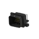
| Description | Automotive Connectors SUPER SEAL 26POS CAP ASSY H AU |
| Datasheet URL | Present |
| Schematic representation | 28 terminals total: 26 signal positions + 2 mounting holes |
| PCB footprint asset | 64734231.kicad_mod |
| 3D model asset | 6473423-1.stp |
Table
| Item | Current project state |
|---|---|
| Signal positions | 26 |
| Mechanical mounting holes | 2 |
| Total pads/terminals | 28 |
| Pin numbering | Numeric positions plus MH1/MH2 for mounting holes |
| Pin names/descriptions | Not defined beyond pad numbers |
| Pin electrical types | Currently Unspecified |
Table
| Category | Datasheet details |
|---|---|
| Part description | SUPER SEAL CONNECTOR (UPPER LOCK) CAP HOUSING 26POS. ASS'Y |
| Drawing number | 9-1437287-8 |
| Connector style | Cap housing assembly / upper lock |
| Number of positions | 26 |
| Housing material | Polyester |
| Arrangement plate material | Polyester |
| Contact material | Brass |
| Contact plating | Gold over Ni on contact area |
| Solder tail plating | Tin-lead over Ni or tin over Ni appears in notes |
Table
| Parameter | Datasheet value |
|---|---|
| Connector length | 39.5 mm |
| Connector width | 36.5 mm |
| Profile height from PCB | 23 mm |
| Mounting-hole span | 32.5 ±0.1 mm |
| Through-hole diameter | Ø1.3 +0.2 mm |
| Mounting-hole diameter | Ø3.3 ±0.1 mm |
Table
| Parameter | Datasheet value |
|---|---|
| Contact pitch reference | 3 mm centerline |
| Additional pitch references | 1.5 pitch, 2.5 ±0.05 mm, 3 ±0.05 mm |
| Hole pattern area | 18 ±0.1 mm by 15 ±0.1 mm |
| Lower mounting-hole vertical reference | 6.5 ±0.1 mm |
Table
| Category | Result |
|---|---|
| Electrical characteristics | Not provided in this drawing |
| Contact current/voltage rating | Not present in this document |
| Insulation resistance | Not present in this document |
| Dielectric withstanding voltage | Not present in this document |
Table
| Category | Result |
|---|---|
| Absolute maximum ratings | Not provided in this drawing |
Table
| Category | Result |
|---|---|
| Operating temperature | Not provided in this drawing |
| Environmental limits | Not provided in this drawing |
Table
| Category | Result |
|---|---|
| Pin function table | Not provided |
| Signal names per cavity | Not provided |
| Cavity numbering | Housing indicates positions, but no full text pin-function table was found |
Table
| Category | Datasheet details |
|---|---|
| Mounting hardware note | JIS B 1122 cross recessed pan head tapping screw |
| Mounting feature | With mounting holes |
| Panel mount feature | Without |
| Mating part note | Mating plug assembly referenced in Table-1 |
| Sealing/color/keying | Not explicitly stated in the retrieved text |
Table
| Check item | Result | Notes |
|---|---|---|
| Signal position count | Pass | Project has 26 signal positions, matching datasheet |
| Mechanical holes | Pass | Project includes 2 mounting holes, matching datasheet |
| Total represented terminals/pads | Pass | 28 total = 26 + 2 mounting holes |
| Pad numbering continuity | Pass | Positions 1-26 are present |
| Mounting hole naming | Pass with caveat | Mechanical holes are clearly separated as MH pads |
| Footprint overall length | Pass | Footprint body outline is 39.5 mm, matching datasheet |
| Mounting-hole span | Pass | Footprint uses 32.5 mm center spacing |
| Mounting-hole drill | Pass | Footprint drill 3.4 mm aligns with datasheet Ø3.3 ±0.1 mm |
| Signal-hole drill | Borderline / acceptable | Footprint drill is 1.5 mm; datasheet gives Ø1.3 +0.2 mm, so 1.5 mm is at the upper limit |
| Contact pattern geometry | Pass | Footprint row/column geometry matches the datasheet pitch pattern |
| Pin descriptions | Incomplete | Datasheet has no pin-function table, so numbered pins are acceptable |
| Symbol electrical pin types | Issue | All are Unspecified |
| Symbol implementation style | Usability issue | Represented as many terminal primitives rather than a richer connector symbol |
Table
| Severity | Finding | Why it matters |
|---|---|---|
| Medium | All symbol pins are Unspecified electrical type | Weak ERC behavior; easier to miss connection issues in downstream designs |
| Medium | Pin entries show undefined pin objects/descriptions | Reduces clarity and increases risk of integration mistakes |
| Low | Datasheet is a customer drawing, not a full electrical spec sheet | Important electrical/environmental limits are missing, so part validation is incomplete |
| Low | Signal-hole drill is set to 1.5 mm, the top end of the stated datasheet range | Likely manufacturable, but leaves no margin if the recommended interpretation was intended to be tighter |
| Low | Symbol is minimal and purely numeric | Fine for a connector with no pin functions, but not ideal for usability |
Table
| Area | Verdict |
|---|---|
| Ordering risk | Low - MPN and mechanical identity are consistent |
| Manufacturing risk | Low to medium - footprint looks mechanically consistent with the drawing |
| Board failure risk from symbol/footprint mismatch | Low based on available evidence |
| Main remaining concern | Missing full electrical/specification data and weak symbol metadata |
Table
| Priority | Improvement |
|---|---|
| 1 | Set pin electrical types for the connector pins and mounting holes |
| 2 | Add pin descriptions such as Position 1 through Position 26 and mark mounting holes as mechanical |
| 3 | Confirm whether 1.5 mm finished drill is your intended fabrication target or whether you want slightly more annular margin based on the mating header lead dimensions |
| 4 | Add a second source document with full product specifications if you need environmental/electrical validation |
If you want, I can next turn this into a punch-list of exact symbol-property fixes to make in the part project.
List symbol fixes
Check DRC/ERC
Find full spec sheet


Welcome 👋
Flux accelerates your PCB design with AI.
Create your account to start using this component and bring your ideas to life.