Part Datasheet Analysis and Verification
1:44
Evalu.
Using Schematic Tool.
Using BOM Tool.
Using PCB Layout Tool.
Looking for "part description, package type, package size, number of terminals, polarity marking, peak wavelength, dominant wavelength, luminous intensity, forward voltage, forward current, reverse voltage, power dissipation, operating temperature, storage temperature, electrostatic discharge, soldering conditions, moisture sensitivity level, thermal resistance, viewing angle, reliability notes, and special features" in 150505RS73300.pdf
Looking for "absolute maximum ratings" in 150505RS73300.pdf
Looking for "electrical characteristics" in 150505RS73300.pdf
Looking for "recommended operating conditions" in 150505RS73300.pdf
Looking for "pin configuration and internal circuit" in 150505RS73300.pdf
Looking for "package information mechanical dimensions" in 150505RS73300.pdf
Looking for "land pattern or recommended pad layout" in 150505RS73300.pdf
Looking for "special features and application notes" in 150505RS73300.pdf
Looking for "mechanical dimensions body length body width body height terminal pitch pad dimensions and terminal dimensions" in 150505RS73300.pdf
Looking for "recommended land pattern dimensions for each pad including pad width pad length row spacing and pitch" in 150505RS73300.pdf
Looking for "terminal numbering order and which pins are cathode and anode" in 150505RS73300.pdf
Looking for "internal circuit 3 chips parallel and electrical meaning of pins 1 through 6" in 150505RS73300.pdf
Assess.
Using Calculator Tool.
Project metadata
| Field | Value |
|---|---|
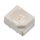
| Description | WL-SMTW SMT Mono-color TOP LED, waterclear, 5050 red |
| MPN | 150505RS73300 |
| Manufacturer | Würth |
| Mount | Surface Mount |
| Part type | Optoelectronic Devices |
| Designator prefix | LED |
| Datasheet | Datasheet |
Schematic symbol state
| Symbol terminal | Mapped pin number | Intended polarity from datasheet | Current symbol metadata |
|---|---|---|---|
| K1 | 1 | Cathode | Pin type = Unspecified, pin name undefined |
| A1 | 2 | Anode | Pin type = Unspecified, pin name undefined |
| K2 | 3 | Cathode | Pin type = Unspecified, pin name undefined |
| A2 | 4 | Anode | Pin type = Unspecified, pin name undefined |
| K3 | 5 | Cathode | Pin type = Unspecified, pin name undefined |
| A3 | 6 | Anode | Pin type = Unspecified, pin name undefined |
Footprint state
| Item | Observed |
|---|---|
| Footprint asset | 150505RS73300.kicad_mod |
| 3D model asset | 150505RS73300.stp |
| Pad count | 6 SMD pads |
| Pad numbering | 1 to 6 |
| Pad size in footprint | 1.0 mm x 2.8 mm |
| Pad row span from copper edge to copper edge | 7.2 mm |
| Package body drawing in datasheet | 5.0 mm x 5.0 mm x 1.6 mm |
General metadata
| Category | Datasheet value |
|---|---|
| Device type | SMT mono-color TOP LED |
| Lens | Waterclear |
| Chip technology | AlInGaP |
| Emitting color | Red |
| Internal structure | 3 LED chips, ratings specified for all 3 chips in parallel circuit |
| Package size | 5050 |
| Dimensions | 5.0 ± 0.1 mm x 5.0 ± 0.1 mm x 1.6 ± 0.1 mm |
| Terminals | 6 |
| Polarity marking | Cathode polarity mark |
| Viewing angle | 120° typ. |
| Compliance | RoHS compliant, REACh conform/declared, halogen-free |
Electrical and optical characteristics
| Parameter | Conditions | Datasheet value |
|---|---|---|
| Peak wavelength λPeak | 60 mA | 630 nm typ. |
| Dominant wavelength λDom | 60 mA | 625 nm typ. |
| Luminous intensity IV | 60 mA | 2050 min / 2300 typ mcd |
| Forward voltage VF | 60 mA | 2.0 typ / 2.4 max V |
| Spectral bandwidth Δλ | 60 mA | 20 nm typ. |
| Reverse current IREV | 5 V | 10 µA max |
| Viewing angle 2θ50% | 60 mA | 120° typ. |
Absolute maximum ratings
| Parameter | Conditions | Datasheet value |
|---|---|---|
| Power dissipation PDiss | Ambient 25 °C | 156 mW |
| Continuous forward current IF | Ambient 25 °C | 65 mA |
| Peak forward current IF,Peak | duty/10 @ 1 kHz | 100 mA |
| Reverse voltage VREV | 5 V | |
| ESD threshold, HBM VESD | 2000 V |
Recommended operating and handling conditions
| Parameter | Datasheet value |
|---|---|
| Operating temperature | -40 to +85 °C |
| Storage, single parts | -40 to +85 °C |
| Storage, original packaging | < 40 °C, < 90 % RH |
| Moisture sensitivity level | MSL 3 |
| Reflow standard | IPC/JEDEC J-STD-020E |
| Reflow cycles | 2 cycles max. |
| Peak package temperature | Depends on package thickness; for < 1.6 mm, 260 °C |
Pin descriptions from the datasheet
| Pin | Function |
|---|---|
| 1 | Cathode of chip 1 |
| 2 | Anode of chip 1 |
| 3 | Cathode of chip 2 |
| 4 | Anode of chip 2 |
| 5 | Cathode of chip 3 |
| 6 | Anode of chip 3 |
Package / land pattern data found
| Item | Datasheet value |
|---|---|
| Body length | 5.0 ± 0.1 mm |
| Body width | 5.0 ± 0.1 mm |
| Body height | 1.6 ± 0.1 mm |
| Terminal dimensions shown | 0.9 ± 0.2 mm, 0.6 ± 0.2 mm |
| Spacing values shown | 3.3 ± 0.2 mm, 1.05 typ., 3.9 typ. |
| Recommended land pattern values shown | 1.6 mm, 2.8 mm, 7.2 mm, 1.0 mm, 4.0 mm, 0.5 mm |
Special features / cautions
| Topic | Datasheet note |
|---|---|
| Assembly | Pad pattern is a general recommendation; high-density applications should optimize it |
| Cleaning | Washing agents may damage body, marking, or plating; brushing is not recommended |
| Potting | Shrink/expansion can damage device or sealing |
| Storage time | Use within 12 months of shipment recommended |
| Handling | Pressure on top surface can affect function and reliability |
| ESD | ESD prevention methods required during handling |
Findings
| Area | Result | Risk | Details |
|---|---|---|---|
| Pin count | Pass | Low | Symbol exposes 6 pins and footprint has 6 pads, matching the datasheet |
| Pin numbering | Pass | Low | Symbol terminal numbers 1-6 align with footprint terminal IDs 1-6 |
| Pin polarity mapping | Pass | Low | K1, K2, K3 map to cathodes; A1, A2, A3 map to anodes, consistent with the datasheet |
| Footprint pad size | Pass | Low | Footprint uses 1.0 x 2.8 mm pads, matching the datasheet land-pattern values |
| Footprint overall pad span | Pass | Low | Copper span is 7.2 mm, matching the datasheet land-pattern value |
| Package family | Pass | Low | Footprint is clearly built for a 5050 6-pad LED package |
| Symbol pin names | Flag | Medium | The symbol metadata shows pin names as undefined; datasheet functions should be explicit as K1/A1/K2/A2/K3/A3 or C1/A1/C2/A2/C3/A3 in the actual pin properties |
| Symbol pin electrical types | Flag | Medium | All pins are currently Unspecified. For ERC clarity and downstream reuse, these should be set explicitly, typically as passive LED terminals or clearly labeled anode/cathode terminals |
| Datasheet property naming | Minor flag | Low | Project property is Datasheet URL. If your library workflow expects a canonical Datasheet field, consistency may matter for automation, but functionally the URL is present |
- No footprint-to-datasheet mismatch was found that would obviously cause manufacturing failure.
- No pin-count or pad-mapping issue was found that would obviously cause incorrect ordering.
- The main issues are symbol metadata quality, not geometry:
- pin names are not formally defined
- pin types are unspecified
Ready.
Reviews

- Wirelessly connects nets on schematic. Used to organize schematics and separate functional blocks. To wirelessly connect net portals, give them same designator. #portaljharwinbarrozo43.0M
- Wirelessly connects power nets on schematic. Identical to the net portal, but with a power symbol. Used to organize schematics and separate functional blocks. To wirelessly connect power net portals, give them the same designator. #portal #powerjharwinbarrozo11.4M
- A generic fixed resistor for rapid developing circuit topology. Save precious design time by seamlessly add more information to this part (value, footprint, etc.) as it becomes available. Standard resistor values: 1.0Ω 10Ω 100Ω 1.0kΩ 10kΩ 100kΩ 1.0MΩ 1.1Ω 11Ω 110Ω 1.1kΩ 11kΩ 110kΩ 1.1MΩ 1.2Ω 12Ω 120Ω 1.2kΩ 12kΩ 120kΩ 1.2MΩ 1.3Ω 13Ω 130Ω 1.3kΩ 13kΩ 130kΩ 1.3MΩ 1.5Ω 15Ω 150Ω 1.5kΩ 15kΩ 150kΩ 1.5MΩ 1.6Ω 16Ω 160Ω 1.6kΩ 16kΩ 160kΩ 1.6MΩ 1.8Ω 18Ω 180Ω 1.8KΩ 18kΩ 180kΩ 1.8MΩ 2.0Ω 20Ω 200Ω 2.0kΩ 20kΩ 200kΩ 2.0MΩ 2.2Ω 22Ω 220Ω 2.2kΩ 22kΩ 220kΩ 2.2MΩ 2.4Ω 24Ω 240Ω 2.4kΩ 24kΩ 240kΩ 2.4MΩ 2.7Ω 27Ω 270Ω 2.7kΩ 27kΩ 270kΩ 2.7MΩ 3.0Ω 30Ω 300Ω 3.0KΩ 30KΩ 300KΩ 3.0MΩ 3.3Ω 33Ω 330Ω 3.3kΩ 33kΩ 330kΩ 3.3MΩ 3.6Ω 36Ω 360Ω 3.6kΩ 36kΩ 360kΩ 3.6MΩ 3.9Ω 39Ω 390Ω 3.9kΩ 39kΩ 390kΩ 3.9MΩ 4.3Ω 43Ω 430Ω 4.3kΩ 43KΩ 430KΩ 4.3MΩ 4.7Ω 47Ω 470Ω 4.7kΩ 47kΩ 470kΩ 4.7MΩ 5.1Ω 51Ω 510Ω 5.1kΩ 51kΩ 510kΩ 5.1MΩ 5.6Ω 56Ω 560Ω 5.6kΩ 56kΩ 560kΩ 5.6MΩ 6.2Ω 62Ω 620Ω 6.2kΩ 62KΩ 620KΩ 6.2MΩ 6.8Ω 68Ω 680Ω 6.8kΩ 68kΩ 680kΩ 6.8MΩ 7.5Ω 75Ω 750Ω 7.5kΩ 75kΩ 750kΩ 7.5MΩ 8.2Ω 82Ω 820Ω 8.2kΩ 82kΩ 820kΩ 8.2MΩ 9.1Ω 91Ω 910Ω 9.1kΩ 91kΩ 910kΩ 9.1MΩ #generics #CommonPartsLibraryjharwinbarrozo1.5M
- A generic fixed capacitor ideal for rapid circuit topology development. You can choose between polarized and non-polarized types, its symbol and the footprint will automatically adapt based on your selection. Supported options include standard SMD sizes for ceramic capacitors (e.g., 0402, 0603, 0805), SMD sizes for aluminum electrolytic capacitors, and through-hole footprints for polarized capacitors. Save precious design time by seamlessly add more information to this part (value, footprint, etc.) as it becomes available. Standard capacitor values: 1.0pF 10pF 100pF 1000pF 0.01uF 0.1uF 1.0uF 10uF 100uF 1000uF 10,000uF 1.1pF 11pF 110pF 1100pF 1.2pF 12pF 120pF 1200pF 1.3pF 13pF 130pF 1300pF 1.5pF 15pF 150pF 1500pF 0.015uF 0.15uF 1.5uF 15uF 150uF 1500uF 1.6pF 16pF 160pF 1600pF 1.8pF 18pF 180pF 1800pF 2.0pF 20pF 200pF 2000pF 2.2pF 22pF 20pF 2200pF 0.022uF 0.22uF 2.2uF 22uF 220uF 2200uF 2.4pF 24pF 240pF 2400pF 2.7pF 27pF 270pF 2700pF 3.0pF 30pF 300pF 3000pF 3.3pF 33pF 330pF 3300pF 0.033uF 0.33uF 3.3uF 33uF 330uF 3300uF 3.6pF 36pF 360pF 3600pF 3.9pF 39pF 390pF 3900pF 4.3pF 43pF 430pF 4300pF 4.7pF 47pF 470pF 4700pF 0.047uF 0.47uF 4.7uF 47uF 470uF 4700uF 5.1pF 51pF 510pF 5100pF 5.6pF 56pF 560pF 5600pF 6.2pF 62pF 620pF 6200pF 6.8pF 68pF 680pF 6800pF 0.068uF 0.68uF 6.8uF 68uF 680uF 6800uF 7.5pF 75pF 750pF 7500pF 8.2pF 82pF 820pF 8200pF 9.1pF 91pF 910pF 9100pF #generics #CommonPartsLibraryjharwinbarrozo1.5M
- A generic fixed inductor for rapid developing circuit topology. *You can now change the footprint and 3D model at the top level anytime you want. This is the power of #genericsjharwinbarrozo15.5k
- An electrical connector acting as reusable interface to a conductor and creating a point where external circuits can be connected.Terminal
- 47 kOhms ±5% 0.125W, 1/8W Chip Resistor 0805 (2012 Metric) Automotive AEC-Q200 Thick Film #forLedBlinkjharwinbarrozo1.2M
- 10uF Capacitor Aluminum Polymer 20% 16V SMD 5x5.3mm #forLedBlink #commonpartslibrary #capacitor #aluminumpolymer #radialcanjharwinbarrozo1.2M
- Yellow 595nm LED Indication - Discrete 1.7V 1206 (3216 Metric) #forLedBlinkjharwinbarrozo1.1M


Pricing & Availability
See prices from popular manufacturers for your project.
Assets
150505RS73300
150505RS73300.stp3D Model
150505RS73300-thumb.png
150505RS73300-thumbThumbnail
150505RS73300
150505RS73300 Symbol.svgDefault150505RS73300
150505RS73300.kicad_modFootprintControls
Welcome 👋
Flux accelerates your PCB design with AI.
Create your account to start using this component and bring your ideas to life.