Memory
RP2040
RP2040 chip for Raspberry Pi Pico - ARM® Cortex®-M0+ MCU 32-Bit The RP2040 is a high-performance, low-cost microcontroller built around two ARM Cortex-M0+ cores. It is optimized for flexibility, ease of use, and deterministic real-time performance. Unlike many microcontrollers, it includes a unique programmable I/O subsystem (PIO), allowing custom hardware interfaces without extra components. Key Features Processing Dual-core ARM Cortex-M0+ processors Up to 133 MHz clock speed Efficient integer performance with low power consumption Memory 264 KB on-chip SRAM External QSPI flash support (typically 2 MB–16 MB depending on board) Programmable I/O (PIO) 2 PIO blocks, each with 4 state machines Enables custom protocols (e.g., SPI, I2C, UART, WS2812, VGA, etc.) Offloads timing-critical tasks from CPU 🔗 Connectivity Interfaces 2× UART 2× SPI 2× I2C USB 1.1 controller (device or host support) 16× PWM channels Analog Features 12-bit ADC (up to 5 channels, including internal temperature sensor) Power & Voltage Operating voltage: 1.8V – 3.3V Low-power modes available Package Options QFN-56 (7×7 mm) Development Ecosystem Supports C/C++ SDK MicroPython and CircuitPython support Strong community and documentation Typical Applications Embedded systems and IoT devices Robotics and automation DIY electronics and prototyping USB devices (HID, MIDI, etc.) Custom communication interfaces using PIO #CommonPartsLibrary #IntegratedCircuit #Microcontroller
1.1k Uses
12 Stars
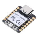
Seeed Studio XIAO RP2040
The Seeed Studio XIAO RP2040 is as small as the Seeed Studio XIAO SAMD21 but it's more powerful. On one hand, it carries the powerful Dual-core RP2040 processor that can flexible clock running up to 133 MHz which is a low-power microcontrollers. On the Seeed Studio XIAO RP2040 there is also 264KB of SRAM, and 2MB of on-board Flash memory which can provide more program to save and run. On the other hand, this little board has good performance in processing but needs less power. All in all, it is designed in a tiny size as small as a thumb(20x17.5mm) and can be used for wearable devices and small projects. #RP2040 #PICO #XIAO #SeedStudio
517 Uses
12 Stars
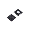
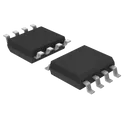
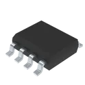
STM32G031J6M6
ARM® Cortex®-M0+ STM32G0 Microcontroller IC 32-Bit Single-Core 64MHz 32KB (32K x 8) FLASH 8-SOIC The STM32G031J6M6 is a compact, low-power 32-bit microcontroller from STMicroelectronics, based on the Arm® Cortex®-M0+ core running at up to 64 MHz. It belongs to the STM32G0 series, designed for cost-sensitive and energy-efficient embedded applications. This MCU integrates essential peripherals, memory, and system functions into a small package (8-pin SOIC), making it suitable for consumer electronics, industrial control, appliances, and IoT devices where space and power efficiency are critical. Key Features Core & Performance 32-bit Arm Cortex-M0+ CPU Up to 64 MHz clock frequency Memory Protection Unit (MPU) for improved reliability and security 💾 Memory 32 KB Flash memory (program storage) 8 KB SRAM Flash protection (read/write protection, secure area) Peripherals & Interfaces Communication: I2C (2x) SPI (2x) / I2S USART (2x) + Low-power UART 12-bit ADC (up to ~2.5 MSps, multiple channels) DMA controller (5 channels) Timers: Advanced PWM timer (motor control capable) General-purpose timers (16-bit & 32-bit) Low-power timers Watchdog timers RTC (Real-Time Clock) with VBAT backup Power & Efficiency Operating voltage: 1.7 V to 3.6 V Multiple low-power modes: Sleep, Stop, Standby, Shutdown Optimized for low energy consumption (battery-powered designs) I/O & Package Up to 44 GPIOs (depending on package) 6 GPIOs available in the 8-pin (J6M6) package 5V-tolerant I/O pins (select pins) Compact SOIC-8 package#commonpartslibrary #integratedcircuit #microcontroller
1.1k Uses
10 Stars
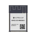
ESP32-S3-WROOM-1U-N16R8
Bluetooth, WiFi 802.11b/g/n, Bluetooth v5.0 Transceiver Module 2.4GHz Antenna Not Included, U.FL Surface Mount The ESP32-S3-WROOM-1U-N16R8 is a high-performance embedded module designed for IoT and edge computing applications, featuring integrated wireless connectivity and enhanced processing capabilities. Processor: Dual-core Xtensa LX7, up to 240 MHz Wireless Connectivity: Wi-Fi 2.4 GHz (802.11 b/g/n) Bluetooth LE 5.0 Memory Configuration (N16R8): 16 MB Flash memory 8 MB PSRAM Antenna Type: U.FL connector for external antenna (“1U” variant) Indicates support for an external antenna via U.FL connector Allows improved RF performance and flexible antenna placement #commonpartslibrary #rf #wireless #transceiver #module
612 Uses
9 Stars
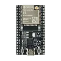
ESP32-DEVKITC-32UE
- ESP32-WROOM-32UE Transceiver; 802.11 b/g/n (Wi-Fi, WiFi, WLAN), Bluetooth® Smart Ready 4.x Dual Mode 2.4GHz Evaluation Board The ESP32-DEVKITC-32UE is a development board based on the ESP32 series SoC designed by Espressif. It is widely used for IoT, embedded systems, and wireless communication applications due to its built-in Wi-Fi and Bluetooth capabilities. Microcontroller: ESP32 dual-core Tensilica LX6 processor Wireless Connectivity: Wi-Fi (802.11 b/g/n) and Bluetooth (Classic + BLE) Flash Memory: Integrated SPI flash (varies by module version) Development Interface: USB-to-UART bridge for easy programming and debugging Power Supply: Typically powered via USB or external 5V input GPIO Pins: Multiple multifunction GPIOs supporting ADC, DAC, PWM, SPI, I2C, UART, etc. Supports deep sleep and ultra-low power modes Multiple peripheral interfaces (SPI, I2C, UART, SDMMC, PWM) Compatible with ESP-IDF, Arduino IDE, and MicroPython Built-in antenna (UE variant uses U.FL or external antenna option depending on module design) IoT devices and smart home systems Wireless sensor networks Data logging and monitoring systems Robotics and automation Embedded control systems #commonpartslibrary #developmentboard #esp32 #wroom
932 Uses
7 Stars
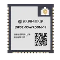
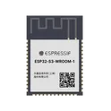
ESP32-S3-WROOM-1-N16R8
Bluetooth, WiFi 802.11b/g/n, Bluetooth v5.0 Transceiver Module 2.4GHz PCB Trace Surface Mount The ESP32-S3-WROOM-1-N16R8 is a high-performance Wi-Fi + Bluetooth Low Energy (BLE) module developed by Espressif Systems. It is built around the ESP32-S3 SoC, featuring a dual-core Xtensa LX7 32-bit processor running up to 240 MHz. This module integrates 16 MB Flash memory and 8 MB PSRAM, making it suitable for memory-intensive applications such as AI, image processing, and advanced IoT systems. It also includes an onboard PCB trace antenna, RF circuitry, crystal oscillator, and power management components—allowing designers to quickly integrate wireless connectivity into compact embedded designs. Key Features Processing & Memory Dual-core Xtensa LX7 CPU, up to 240 MHz 384 KB ROM, 512 KB SRAM + 16 KB RTC SRAM 16 MB Flash (Quad SPI) 8 MB PSRAM (Octal/Quad SPI) Connectivity 2.4 GHz Wi-Fi (802.11 b/g/n) Bluetooth 5 (LE) + Mesh support Integrated PCB antenna Peripherals & Interfaces Up to 36 GPIOs Interfaces: UART, SPI, I2C, I2S, PWM, ADC, USB OTG Built-in USB Serial/JTAG support Supports touch sensors, timers, watchdogs, CAN (TWAI) Electrical Characteristics Supply voltage: 3.0 V – 3.6 V TX power: up to ~20.5 dBm RX sensitivity: ~-103.5 dBm Operating temp: −40 °C to +65 °C (typical) Advanced Capabilities Optimized for AI acceleration (vector instructions) Suitable for voice recognition, image processing, and edge AI Low-power modes for battery-operated devices| Typical Applications IoT devices and sensor hubs Smart home & home automation AIoT (voice/image recognition) Industrial automation & monitoring Wearables and health devices USB-connected embedded systems #Module #RF-Transceiver #ESP32-S3
1.9k Uses
5 Stars
ESP32-S3-WROOM-1-N16R8
The ESP32-S3-WROOM-1-N16R8 is a high-performance Wi-Fi and Bluetooth Low Energy (BLE) module from Espressif Systems, built around the ESP32-S3 SoC. It integrates a dual-core Xtensa® LX7 processor running at up to 240 MHz, along with 16 MB Quad SPI Flash and 8 MB Octal SPI PSRAM, making it suitable for memory-intensive embedded, IoT, AIoT, multimedia, and edge AI applications. The module includes an onboard PCB antenna, RF matching circuitry, crystal oscillator, and flash/PSRAM, simplifying hardware design and reducing development time. Key Features Dual-core Xtensa LX7 CPU operating up to 240 MHz 16 MB onboard Flash memory 8 MB onboard Octal PSRAM for large buffers, graphics, and AI workloads 2.4 GHz Wi-Fi (IEEE 802.11 b/g/n) Bluetooth 5.0 Low Energy (BLE) Built-in support for AI acceleration and vector instructions for machine learning and signal processing applications Rich peripheral set including: GPIO UART SPI I²C I²S USB 2.0 OTG PWM ADC Touch sensing SD/MMC interface CAN (TWAI) Integrated USB Serial/JTAG debugging capability Supply voltage range: 3.0 V to 3.6 V Operating temperature: −40°C to +65°C Surface-mount module with integrated PCB antenna Supports secure boot, flash encryption, and hardware cryptographic acceleration for secure IoT devices. Typical Applications Smart home and IoT devices Edge AI and machine learning Voice assistants and speech recognition Industrial automation Human-machine interfaces (HMI) Wireless sensors and gateways Smart displays and touch panels Audio streaming and multimedia devices Robotics and connected products #RF-Transceiver #Module #ESP32
223 Uses
3 Stars