Battery Management ICs
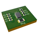
STC3115 Module
This project is a Battery Management System (BMS) built around STMicroelectronics' STC3115AIQT battery monitor IC. It uses I2C for communication, features alarm management, and supports battery charging. The power supply, battery connection points, and debug interface are facilitated through connectors. #project #Template #charger #monitor #reusable #module #batterycharger #template #bms #STC3115 #stm
13 Uses
2 Stars
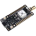
Seeed Studio Wio-E5 mini Dev Board
Wio-E5 mini Dev Board builds in and leads out full GPIO of the Wio-E5 STM32WLE5JC LoRa module. Supporting Long Range protocol and global frequency, the Wio-E5 mini is able to achieve a transmission range of up to 10 km in open areas. It supports EU868 and US915, making it suitable for wireless sensor networks and other IoT devices that require battery power, low power consumption and long range.
10 Uses
2 Stars
STM32MP257FAI3
MPU with Dual Arm Cortex-A35 @1.5GHz, Cortex-M33 @400MHz, 3xEthernet (2+1 switch), 3xFD-CAN, LVDS/DSI, H.264, 3D GPU, AI/NN, Secure Boot, Cryptography, DRAM enc/dec, PKA The STM32MP257FAI3 is a high-performance microprocessor from STMicroelectronics' STM32MP2 series, integrating dual 64-bit Arm Cortex-A35 cores running at up to 1.5 GHz, a Cortex-M33 real-time core, and a Cortex-M0+ low-power management core. It is designed for advanced industrial, edge AI, machine vision, HMI, IoT gateway, and multimedia applications requiring Linux-class processing alongside deterministic real-time control. The device features AI acceleration, 3D graphics, video encoding/decoding, extensive connectivity, advanced security, and support for high-speed external memory. Key Features Dual-core 64-bit Arm Cortex-A35 CPU operating up to 1.5 GHz Arm Cortex-M33 real-time processor with TrustZone and FPU support Arm Cortex-M0+ low-power coprocessor for autonomous operation Integrated NPU (Neural Processing Unit) delivering up to 1.35 TOPS AI performance 3D GPU and hardware video encoder/decoder acceleration Supports DDR3L, DDR4, and LPDDR4 external memory up to 4 GB Multiple display interfaces including MIPI-DSI, LVDS, and parallel RGB USB 2.0 Host and USB 3.0 Dual-Role with embedded PHYs PCI Express interface with integrated 5 Gbps PHY Up to three Gigabit Ethernet interfaces with TSN and IEEE 1588 support Extensive connectivity: I2C, I3C, SPI, UART, USART, CAN FD, SDMMC, SAI, and SPDIF Hardware cryptographic accelerators including AES, SHA, RSA, ECC, PKA, and True RNG Secure boot, TrustZone security, tamper detection, and resource isolation framework Multiple low-power operating modes for energy-efficient designs Available in fine-pitch BGA packages for high-density embedded systems. #STM32MP257FAI3 #STM32MP2 #STMicroelectronics #CortexA35 #CortexM33 #EdgeAI #EmbeddedLinux #IndustrialAutomation #MachineVision #HMI #IoTGateway #MPU #PCIe #USB3 #GigabitEthernet #TrustZone #EmbeddedSystems #ArtificialIntelligence #LinuxProcessor #IndustrialIoT #CommonPartsLibrary #IntegratedCircuit #Microprocessor #STM32MP2
32 Uses
1 Star
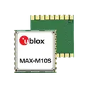
MAX-M10S-00B
MAX-M10 RF Receiver BeiDou, Galileo, GLONASS, GPS, GNSS 1.561GHz, 1.575GHz, 1.602GHz -167dBm 921.6kbps Not Included Module The MAX-M10S-00B is a professional-grade, ultra-low-power GNSS positioning module from u-blox based on the u-blox M10 platform. It is designed for battery-powered applications such as asset trackers, wearables, IoT devices, and navigation systems. The module supports simultaneous reception of multiple GNSS constellations, providing high positioning availability, fast acquisition times, and excellent sensitivity even in challenging urban or weak-signal environments. It integrates a TCXO, LNA, and SAW filter to improve RF performance while maintaining very low power consumption. Key Features Multi-constellation GNSS receiver: GPS Galileo GLONASS BeiDou QZSS SBAS support (WAAS, EGNOS, MSAS, GAGAN) Concurrent tracking of up to four GNSS constellations for improved position availability and accuracy. Ultra-low power consumption: Approximately 25 mW in continuous tracking mode, making it ideal for battery-powered devices. High RF sensitivity: Tracking sensitivity up to −167 dBm for reliable operation in weak-signal conditions. High positioning accuracy: Typical position accuracy of approximately 1.5 m CEP under suitable conditions. Navigation update rate: Up to 10 Hz for responsive tracking applications. Integrated RF front-end: Built-in LNA (Low Noise Amplifier) Built-in SAW filter Integrated TCXO for stable operation. Supports Assisted GNSS services: AssistNow Online AssistNow Offline AssistNow Autonomous CloudLocate support for low-power IoT positioning. Communication interfaces: UART I²C NMEA and UBX protocols supported. Wide operating temperature range: −40°C to +85°C. Supply voltage: 1.76 V to 3.6 V. Typical Applications Asset tracking devices Wearable electronics Fleet management systems Industrial IoT Smart meters Drone and robotics navigation Personal navigation devices Timing and synchronization systems Package Information Package Type: Surface-mount LCC module Dimensions: 9.7 mm × 10.1 mm × 2.5 mm (typical module size) #Commonpartslibrary #RF #Wireless #RFreceivers #MAXM10S #uBlox #GNSS #GPS #Galileo #GLONASS #BeiDou #QZSS #NavigationModule #GNSSModule #GPSTracking #AssetTracking #IoT #IndustrialIoT #WearableTech #FleetManagement #DroneNavigation #EmbeddedSystems #ElectronicsDesign #PCBDesign #HardwareEngineering #LowPowerDesign #LocationTracking #Geolocation #RFDesign #LNA #SMTModule
243 Uses
1 Star
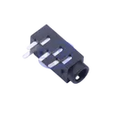
PJ-320A
The PJ-320A is a panel-mount or PCB-mount DC barrel power jack connector designed for low-voltage DC power input applications in embedded and consumer electronic systems. This connector provides a reliable interface for external DC power adapters and is commonly used in development boards, communication devices, industrial electronics, portable equipment, and power distribution modules. The connector is engineered for stable mechanical retention and consistent electrical contact performance during repeated insertion and removal cycles. Its compact construction and standardized barrel interface support broad compatibility with common DC plug adapters used in low-voltage electronic systems. The PJ-320A is widely implemented in embedded hardware, battery charging systems, portable electronics, instrumentation equipment, and microcontroller-based applications requiring secure external power connectivity. Its durable housing and solderable terminal structure support reliable PCB integration and automated assembly processes. Engineering Specification Device Type DC barrel power jack connector Connector Function External DC power input interface Mounting Style PCB mount or panel mount depending on implementation Connector Configuration Coaxial barrel-style power connector Electrical Characteristics Designed for low-voltage DC power transmission Contact Structure Spring-contact conductive interface for stable plug retention Mechanical Features Durable insertion and extraction cycle performance Housing Material Insulated high-strength connector body Terminal Configuration Solderable PCB terminal interface Reliability Features Stable contact resistance and secure mechanical retention Assembly Compatibility Suitable for automated and manual PCB assembly processes Package Structure Compact embedded connector form factor Applications Embedded systems Portable electronics Power adapter interfaces Microcontroller development boards Battery charging systems Industrial electronics Consumer devices Communication equipment Instrumentation systems Low-voltage DC power distribution Manufacturer Commonly associated with generic DC power connector manufacturers #commonpartslibrary #dcjack #powerconnector #barreljack #embeddedhardware #electronicsdesign #powerelectronics #pcbconnectors #consumerelectronics #surfacemountcomponents #throughholecomponents #powerinput #industrialelectronics #microcontroller #electromechanical
80 Uses
1 Star
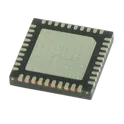
S32K344EHT1VPBST
ARM® Cortex®-M7 S32K3 Microcontroller IC 32-Bit 160MHz 4MB (4M x 8) FLASH 172-QFP (16x16) S32K344EHT1VPBST is an automotive-grade 32-bit microcontroller from NXP Semiconductors based on the Arm Cortex-M7 core architecture. The device is designed for high-performance real-time automotive body, chassis, powertrain, and domain control applications requiring functional safety, security, and advanced communication interfaces. It integrates high-speed processing capability, extensive peripheral integration, hardware security acceleration, and deterministic control functions suitable for safety-critical embedded systems. The microcontroller operates with an Arm Cortex-M7 CPU core running at high frequency with floating-point support and DSP extensions for computationally intensive applications. Integrated flash memory and SRAM provide embedded program and data storage optimized for automotive embedded control systems. The device supports hardware-assisted security features including secure boot, cryptographic acceleration, and tamper protection for secure automotive network communication and firmware integrity. The S32K344EHT1VPBST includes multiple communication peripherals supporting CAN FD, FlexCAN, LIN, SPI, UART, I2C, and Ethernet interfaces for distributed automotive networking and gateway applications. Advanced analog integration includes ADC modules, timers, PWM generators, watchdogs, and motor-control-oriented peripherals enabling precision sensing and control functionality. The device supports functional safety development aligned with ISO 26262 requirements and includes error correction, memory protection, fault monitoring, and safety management features. Power management functionality supports low-power operating modes for energy-efficient automotive electronic control units. The microcontroller is housed in a thermally enhanced LQFP package suitable for automotive operating environments with extended temperature capability and AEC-Q100 qualification for automotive reliability standards. #commonpartslibrary #integratedcircuit #microcontroller #arm #m7
2 Uses
1 Star
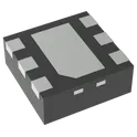
TMP117AIDRVR
Temperature Sensor Digital, Local -55°C ~ 150°C 16 b 6-WSON (2x2) The TMP117AIDRVR is a high-precision digital temperature sensor manufactured by Texas Instruments. The device provides accurate temperature measurements through an I²C-compatible digital interface and is optimized for applications requiring medical-grade accuracy, low power consumption, and compact PCB footprint. The sensor integrates a precision temperature sensing element, analog-to-digital converter, calibration memory, and digital interface into a single compact package. The device supports continuous conversion and shutdown operating modes, enabling efficient thermal monitoring in battery-powered and always-on systems. Internal calibration minimizes external component requirements while providing highly linear and repeatable temperature measurements across an extended operating range. The TMP117AIDRVR is commonly used in industrial controls, wearable electronics, healthcare equipment, environmental monitoring systems, battery management systems, consumer electronics, and precision instrumentation. Electrical Characteristics Supply voltage supports low-voltage digital systems and portable electronics applications. Ultra-low operating current enables long battery life in energy-sensitive designs. Integrated EEPROM allows programmable offset correction and configuration storage. Digital output eliminates the need for external ADC circuitry. High measurement resolution supports precision thermal monitoring applications. Low self-heating characteristics improve measurement stability and accuracy. Functional Features High-accuracy digital temperature sensing. I²C and SMBus compatible communication interface. Programmable alert functionality for thermal threshold monitoring. Continuous conversion and low-power shutdown operating modes. Integrated non-volatile memory for user configuration storage. Wide operating temperature range for industrial and commercial environments. Fast conversion timing suitable for real-time monitoring systems. Factory-calibrated performance requiring minimal external calibration. Package Information Package type is WSON with compact surface-mount footprint suitable for dense PCB layouts. Moisture-sensitive package designed for automated assembly processes. Lead-free and RoHS-compliant construction. Typical Applications Medical thermometers and patient monitoring systems. Industrial temperature monitoring equipment. Battery-powered portable electronics. HVAC and environmental sensing systems. Data acquisition and instrumentation systems. Server and embedded thermal management applications. Consumer electronics requiring precision thermal sensing. #commonpartslibrary #integratedcircuit #temperaturesensor
287 Uses
1 Star