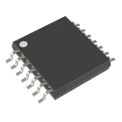
Part Datasheet Review and Verification
Worked for 1 min 29 sec
Review complete. The symbol has the correct 14 pins and pin-number mapping for TI SN74LVC11APWR, but all terminal pin types are still
Unspecified and pin descriptions are missing; the footprint has 14 pads, but exposed layout data didn’t include enough pad geometry to numerically confirm the TI PW0014A land pattern.I created the full report here: SN74LVC11APWR Part Datasheet Review. Suggested next steps: update pin types/descriptions, replace the uploaded datasheet URL with the official TI URL, and verify the TSSOP-14 pad geometry against TI’s recommended land pattern.

Update the pin types/descriptions, switch to the official TI datasheet URL, then run a review.
Thought for 8 sec
I’ll update the terminal metadata from the TI pin table, switch the part datasheet link to TI’s official PDF if the property tool allows it, then run a design review to catch remaining issues.
Worked for 49 sec
Pin metadata is updated and the Datasheet URL now points to TI’s official PDF. I’m running the part review checks next.
Worked for 36 sec
Updated all 14 terminal pin types and pin descriptions from the TI datasheet, and switched the project
Datasheet URL to the official TI PDF: https://www.ti.com/lit/ds/symlink/sn74lvc11a.pdf.Review ran successfully: no matching ERROR/WARNING/UNCERTAIN/OPEN/INFORMATIONAL part-review or missing-footprint issues were reported.
Fix metadata and verify
Set Terminal Types
Verify footprint geometry
Update review report
Prepare for publishing
Refine this doc
Ask about this doc
SN74LVC11APWR Part Datasheet Review
Source information reviewed
- Project MPN:
SN74LVC11APWR - Manufacturer: Texas Instruments
- Project package/case:
14-TSSOP - Project description: Triple 3-input positive-AND gate, 1.1 V to 3.6 V supply, 5.5 V tolerant inputs, ±24 mA drive at 3.3 V, -40 °C to 125 °C, PW/TSSOP-14.
- Existing Datasheet URL property:
https://storage.googleapis.com/graviton-electric-symbols/document_assets/user-uploaded/dfa4a777c9d118f783af00e9c4a76d7cd40106c2046f039371b486c03d785c42.pdf - Official TI datasheet found:
https://www.ti.com/lit/ds/symlink/sn74lvc11a.pdf
Note: The project already had a datasheet URL set, so no mandatory datasheet-property update was required by the request. The existing URL appears to be an uploaded copy rather than the official TI URL.
Key datasheet specs
- Function: Three independent 3-input AND gates, positive logic,
Y = A × B × C. - Supply voltage, recommended: 1.1 V to 3.6 V.
- Input voltage: 5.5 V tolerant inputs.
- Operating free-air temperature: -40 °C to 125 °C.
- Output current, recommended: ±4 mA at 1.8 V, ±8 mA at 2.3 V, ±12 mA at 2.7 V, ±24 mA at 3.0 V.
- Ioff partial-power-down support: max ±10 µA with VCC = 0 V.
- Typical input capacitance: 4.9 pF at 3.3 V.
- Propagation delay, A/B/C to Y: typical 4.1 ns at 3.3 V ±0.3 V, CL = 50 pF; typical 12 ns and max 23 ns at 1.2 V ±0.1 V, CL = 15 pF.
- Package: TI PW0014A / 14-pin TSSOP, JEDEC MO-153, 0.65 mm pitch, 1.2 mm max height.
- Package body: 4.9 mm to 5.1 mm length, 4.3 mm to 4.5 mm body width, 6.2 mm typical to 6.6 mm overall width.
- Recommended land pattern: 14 pads, 0.45 mm × 1.5 mm, 0.65 mm pitch, 5.8 mm overall land-pattern span, non-solder-mask-defined preferred.
Datasheet pin table vs schematic terminals
Table
| Pin | Datasheet signal | Datasheet type | Project terminal | Result |
|---|---|---|---|---|
| 1 | 1A | Input | 1A | Match |
| 2 | 1B | Input | 1B | Match |
| 3 | 2A | Input | 2A | Match |
| 4 | 2B | Input | 2B | Match |
| 5 | 2C | Input | 2C | Match |
| 6 | 2Y | Output | 2Y | Match |
| 7 | GND | Ground | GND | Match |
| 8 | 3Y | Output | 3Y | Match |
| 9 | 3A | Input | 3A | Match |
| 10 | 3B | Input | 3B | Match |
| 11 | 3C | Input | 3C | Match |
| 12 | 1Y | Output | 1Y | Match |
| 13 | 1C | Input | 1C | Match |
| 14 | VCC | Power | VCC | Match |
Symbol review
- Pin count is correct: 14 terminals present.
- Pin numbers and signal names match the TI datasheet pinout for D/PW top view.
- Symbol orientation is generally logical: inputs mostly on the left, outputs on the right, VCC top, GND bottom.
- Mismatch / quality issue: every terminal currently has
Pin Type: Unspecified; datasheet types should be Input, Output, Power, or Ground. - Mismatch / quality issue: terminal-level
Pin Descriptionproperties are not populated; datasheet descriptions should be added for clarity.
Footprint review
- The project footprint contains 14 pad nodes named for the 14 terminals, which matches the TSSOP-14 pin count.
- Silkscreen outline visually resembles a small-outline/TSSOP footprint.
- Footprint verification is incomplete from available layout data: pad geometry values were not exposed by the inspection output, so I could not numerically confirm 0.65 mm pitch, 0.45 mm × 1.5 mm pad size, 5.8 mm land-span, or pin-1 marker location against TI PW0014A.
Mismatches / open items
- Existing
Datasheet URLis an uploaded PDF copy, not the official TI URL. Official URL found:https://www.ti.com/lit/ds/symlink/sn74lvc11a.pdf. - Terminal
Pin Typeproperties are allUnspecified; they should be corrected to Input/Output/Power/Ground according to the pin table. - Terminal
Pin Descriptionproperties are missing; add per-pin channel/input/output descriptions from the datasheet. - Footprint has correct pad count, but exact pad geometry could not be confirmed from exposed layout data. It should be checked against TI PW0014A recommended land pattern before publishing/manufacturing.
Source information reviewed
Key datasheet specs
Datasheet pin table vs schematic terminals
Symbol review
Footprint review
Mismatches / open items