Part Review and Datasheet Update
Worked for 2 mins 9 sec
Completed the requested terminal sectioning: all 74 terminals now have functional
Section and Terminal Order properties, with Power first and Ground last. I also created the requested Flux tables in nRF52840-QIAA-T Terminal Section Table (nrf52840-qiaa-t-terminal-section-table), including grouped section blocks and notes for P0.05/AIN3 and VSS_PA.
Read the file and follow all instructions.
Thought for 4 sec
I’ll read the attached instructions, apply them to the part, and verify the result.
Worked for 2 mins 33 sec
Completed the requested review and saved the tables in
nRF52840-QIAA-T Terminal Section Check (nrf52840-qiaa-t-terminal-section-check). Current terminal sectioning is consistent; rename recommendations are P0.05 → P0.05__AIN3 and VSS_P → VSS_PA.Fix names, validate part
Fix terminal names
Add pin descriptions
Validate part data
Update review documents
Refine this doc
Ask about this doc
nRF52840-QIAA-T Part Review
Reviewed project / part
- Project:
silicon-yard/nrf52840-qiaa-t - Published part UID:
aea5f379-2011-4dec-90ff-f60c1b3d78c6 - MPN:
nRF52840-QIAA-T - Manufacturer: Nordic Semiconductor
- Project description: RF System on a Chip - SoC BLE ANT 2.4GHz SOC
- Part type property: Integrated Circuits
- Designator prefix:
IC - Terminal / pad count in Flux: 74 schematic terminals and 74 footprint pads
Datasheet status
- Existing Datasheet URL property was already set:
http://www.mouser.com/ds/2/297/nRF52840_OPS_v0.5-1074816.pdf - I did not find a missing Datasheet property to populate; therefore no datasheet property update was required by the user instruction.
- Quality note: the stored URL is an older Mouser-hosted Nordic Objective Product Specification v0.5 and uses HTTP. Prefer updating to HTTPS and, if available, Nordic’s current product specification from nordicsemi.com for final release validation.
- HTTPS equivalent of current stored source:
https://www.mouser.com/ds/2/297/nRF52840_OPS_v0.5-1074816.pdf
Key datasheet specs captured
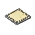
- Package / order code: QI = AQFN 7 mm × 7 mm, 73 pins, 0.5 mm pitch; AA = 1024 kB Flash, 256 kB RAM; T = tray packing.
- Core: Arm Cortex-M4F, 64 MHz.
- Radio: 2.4 GHz multiprotocol radio, BLE 1 Mbps/2 Mbps/long range 125 kbps and 500 kbps, IEEE 802.15.4 250 kbps, Nordic proprietary 1 Mbps/2 Mbps.
- Memory: 1 MB Flash, 256 kB RAM.
- USB: Full-speed 12 Mbps USB controller.
- NFC: NFC-A tag interface.
- Security: Arm CryptoCell 310.
- ADC: 12-bit, 200 kSPS.
- Supply ranges: VDD 1.7–3.6 V; VDDH 2.5–5.5 V; VBUS 4.35–5.5 V.
- Operating temperature: −40 °C to +85 °C.
- RF: single-ended antenna connection at ANT.
- Package dimensions from cited datasheet: D/E nominal 7.00 mm; exposed/die pad D2/E2 nominal 4.85 mm; pad pitch nominal 0.5 mm; terminal b nominal 0.25 mm.
Symbol / pin assignment cross-check
The schematic is modeled as individual
Terminal components rather than a single monolithic IC symbol. Each terminal has a Pin Number property corresponding to the AQFN grid coordinate or die pad.Confirmed matches
The observed Flux terminal pin numbers match the datasheet QIAA pin assignment list for all critical groups checked:
- Power: VDD at A22, B1, W1, AD14, AD23; VDDH at Y2; VBUS at AD2.
- Ground / RF ground: VSS at B7, VSS_PA at F23, exposed die pad VSS at DP1.
- USB: D− at AD4, D+ at AD6.
- SWD: SWDCLK at AA24, SWDIO at AC24.
- RF: ANT at H23.
- LF/HF crystal pins: P0.00/XL1 at D2, P0.01/XL2 at F2, XC1 at B24, XC2 at A23.
- NFC: P0.09/NFC1 at L24, P0.10/NFC2 at J24.
- DEC/DCDC/USB regulator pins: DEC1 C1, DEC2 A18 and E24, DEC3 D23, DEC4 B5, DEC5 N24, DECUSB AC5, DCC B3, DCCH AB2.
- GPIO banks P0 and P1 pin-number assignments otherwise align with the datasheet list reviewed.
Symbol / pin-description issues flagged
P0.05at K2 is missing the alternate analog labelAIN3; datasheet lists this asP0.05/AIN3. This is a naming/description omission, not a pin-number mismatch.VSS_Pat F23 likely representsVSS_PA; the terminal name is truncated/ambiguous. Pin number is correct, but the symbol label should beVSS_PAto match the datasheet.- All terminal
Pin Typeproperties areUnspecified. For a reusable published IC part, these should be refined: power inputs for VDD/VDDH/VBUS, ground for VSS/VSS_PA/DP1, bidirectional/digital/analog-capable for GPIO, signal for RF/USB/crystal pins, etc. - No terminal-level
Pin Descriptionproperties were visible. Adding descriptions would improve downstream schematic readability and ERC behavior.
Footprint cross-check
Footprint asset:
nRF52840QIAAT.kicad_mod, description AQFN73.Confirmed footprint items
- Footprint outline: 7.0 mm × 7.0 mm fab outline, matching AQFN73 7 × 7 mm package.
- Pad count: 73 perimeter/grid pads plus 1 exposed die pad = 74 footprint pads, consistent with Flux terminal count and datasheet die pad.
- Pad pitch / locations: visible pad coordinates step at 0.5 mm increments, matching 0.5 mm pitch.
- Perimeter/grid pad size: 0.300 mm circular pads; datasheet terminal b max is 0.30 mm, so nominal pad size is plausible for an AQFN land pattern.
- Exposed pad: DP1 rectangular pad 4.950 mm × 4.950 mm. Datasheet D2/E2 max is 4.95 mm and nominal is 4.85 mm.
- Pad names in the KiCad footprint match the AQFN grid coordinates from the datasheet, including A8 through AD23 and DP1.
Footprint issues / risks flagged
- Exposed pad size uses 4.95 mm, matching the maximum exposed pad dimension rather than the nominal 4.85 mm. This may be acceptable for a raw package pad model but should be checked against Nordic’s recommended PCB land pattern before production.
- The footprint asset includes circular SMD pads for all package pads. Since AQFN wettable/land pattern recommendations can differ from raw terminal geometry, confirm against the official Nordic/IPC land pattern before fabrication.
- Flux computed footprint
packageSizeappears as zero in the layout tree even though the embedded KiCad footprint has a correct 7 mm fab outline. This may be a metadata omission rather than a geometry error.
Library metadata observations
- The Flux library also contains LCSC-imported variants for
NRF52840-QIAA-Twith packageAQFN-73_L7.0-W7.0-P0.50-BL-EP4.8, LCSCC3007766, JLCPCB Extended Part, but those library entries report no datasheet and manufacturer asOther/NORDIC. - Current Silicon Yard part has a datasheet URL and manufacturer property, but lacks richer structured electrical specs and pin types.
- Library search flagged lifecycle status as
NRNDfor the LCSC entries. Verify lifecycle directly with Nordic before selecting this part for a new production design.
Recommended corrections
- Rename terminal
P0.05toP0.05__AIN3or add a pin descriptionP0.05/AIN3. - Rename terminal
VSS_PtoVSS_PAor add a pin description clarifyingVSS_PA. - Populate terminal
Pin TypeandPin Descriptionproperties for all terminals. - Replace/augment the Datasheet URL with Nordic’s current official HTTPS product specification if available; at minimum switch current URL to HTTPS.
- Validate the footprint against Nordic’s current recommended PCB land pattern before manufacturing, especially exposed pad size/paste segmentation and pad shape.
Reviewed project / part
Datasheet status
Key datasheet specs captured
Symbol / pin assignment cross-check
Confirmed matches
Symbol / pin-description issues flagged
Footprint cross-check
Confirmed footprint items
Footprint issues / risks flagged
Library metadata observations
Recommended corrections