Pad Type Differences Explained
185 days
what is the difference between smd, hold, std and conn in pad type
Thought for 1 min 5 sec
185 days
Here’s what the Flux documentation says about Pad Type options:
"Pad Type
Modifies the type of pad to one of the following:
- SMD – a surface mount pad with no drill hole.
- HOLE – a drill hole with no copper.
- STD – a through-hole pad. (STD stands for "Standard".)
- CONN – a connector pad with no drill hole, often used at the edges of a board."
When to use HOLE
Choosing CONN vs SMD
STD pad design details
Library footprint consistency
Mixed pad types on part
S_R
BAT+
D3
5V
D18
D15
D10
D16
D7
D12
D2
D8
D17
M_CLK
D14
D4
M_R
D0
BAT-
D6
3V3
S_DIO
3V3
D13
GND
D9
D5
GND
M_DIO
S_CLK
D11
D1
Reviews
 A generic fixed inductor suitable for rapid circuit topology development. The footprint automatically adapts based on the selected package, supporting standard SMD sizes (e.g., 0402, 0603, 0805) as well as well-known inductor packages such as SDR1806, PA4320, SRN6028, and SRR1260. Standard inductor values: 1.0 nH, 10 nH, 100 nH, 1.0 µH, 10 µH, 100 µH, 1.0 mH 1.2 nH, 12 nH, 120 nH, 1.2 µH, 12 µH, 120 µH, 1.2 mH 1.5 nH, 15 nH, 150 nH, 1.5 µH, 15 µH, 150 µH, 1.5 mH 1.8 nH, 18 nH, 180 nH, 1.8 µH, 18 µH, 180 µH, 1.8 mH 2.2 nH, 22 nH, 220 nH, 2.2 µH, 22 µH, 220 µH, 2.2 mH 2.7 nH, 27 nH, 270 nH, 2.7 µH, 27 µH, 270 µH, 2.7 mH 3.3 nH, 33 nH, 330 nH, 3.3 µH, 33 µH, 330 µH, 3.3 mH 3.9 nH, 39 nH, 390 nH, 3.9 µH, 39 µH, 390 µH, 3.9 mH 4.7 nH, 47 nH, 470 nH, 4.7 µH, 47 µH, 470 µH, 4.7 mH 5.6 nH, 56 nH, 560 nH, 5.6 µH, 56 µH, 560 µH, 5.6 mH 6.8 nH, 68 nH, 680 nH, 6.8 µH, 68 µH, 680 µH, 6.8 mH 8.2 nH, 82 nH, 820 nH, 8.2 µH, 82 µH, 820 µH, 8.2 mH #generics #CommonPartsLibraryjharwinbarrozo16.4k
- A generic fixed capacitor ideal for rapid circuit topology development. You can choose between polarized and non-polarized types, its symbol and the footprint will automatically adapt based on your selection. Supported options include standard SMD sizes for ceramic capacitors (e.g., 0402, 0603, 0805), SMD sizes for aluminum electrolytic capacitors, and through-hole footprints for polarized capacitors. Save precious design time by seamlessly add more information to this part (value, footprint, etc.) as it becomes available. Standard capacitor values: 1.0pF, 10pF, 100pF, 1000pF, 0.01uF, 0.1uF, 1.0uF, 10uF, 100uF, 1000uF, 10000uF 1.1pF, 11pF, 110pF, 1100pF 1.2pF, 12pF, 120pF, 1200pF 1.3pF, 13pF, 130pF, 1300pF 1.5pF, 15pF, 150pF, 1500pF, 0.015uF, 0.15uF, 1.5uF, 15uF, 150uF, 1500uF 1.6pF, 16pF, 160pF, 1600pF 1.8pF, 18pF, 180pF, 1800pF 2.0pF, 20pF, 200pF, 2000pF 2.2pF, 22pF, 220pF, 2200pF, 0.022uF, 0.22uF, 2.2uF, 22uF, 220uF, 2200uF 2.4pF, 24pF, 240pF, 2400pF 2.7pF, 27pF, 270pF, 2700pF 3.0pF, 30pF, 300pF, 3000pF 3.3pF, 33pF, 330pF, 3300pF, 0.033uF, 0.33uF, 3.3uF, 33uF, 330uF, 3300uF 3.6pF, 36pF, 360pF, 3600pF 3.9pF, 39pF, 390pF, 3900pF 4.3pF, 43pF, 430pF, 4300pF 4.7pF, 47pF, 470pF, 4700pF, 0.047uF, 0.47uF, 4.7uF, 47uF, 470uF, 4700uF 5.1pF, 51pF, 510pF, 5100pF 5.6pF, 56pF, 560pF, 5600pF 6.2pF, 62pF, 620pF, 6200pF 6.8pF, 68pF, 680pF, 6800pF, 0.068uF, 0.68uF, 6.8uF, 68uF, 680uF, 6800uF 7.5pF, 75pF, 750pF, 7500pF 8.2pF, 82pF, 820pF, 8200pF 9.1pF, 91pF, 910pF, 9100pF #generics #CommonPartsLibraryjharwinbarrozo1.5M
- A generic fixed resistor ideal for rapid circuit topology development. Its footprint automatically adapts based on the selected package case code—supporting 0402, 0603, 0805, 1203, and many other standard SMD packages, as well as axial horizontal and vertical configurations. Save precious design time by seamlessly add more information to this part (value, footprint, etc.) as it becomes available. Standard resistor values: 1.0 ohm, 10 ohm, 100 ohm, 1.0k ohm, 10k ohm, 100k ohm, 1.0M ohm 1.1 ohm, 11 ohm, 110 ohm, 1.1k ohm, 11k ohm, 110k ohm, 1.1M ohm 1.2 ohm, 12 ohm, 120 ohm, 1.2k ohm, 12k ohm, 120k ohm, 1.2M ohm 1.3 ohm, 13 ohm, 130 ohm, 1.3k ohm, 13k ohm, 130k ohm, 1.3M ohm 1.5 ohm, 15 ohm, 150 ohm, 1.5k ohm, 15k ohm, 150k ohm, 1.5M ohm 1.6 ohm, 16 ohm, 160 ohm, 1.6k ohm, 16k ohm, 160k ohm, 1.6M ohm 1.8 ohm, 18 ohm, 180 ohm, 1.8K ohm, 18k ohm, 180k ohm, 1.8M ohm 2.0 ohm, 20 ohm, 200 ohm, 2.0k ohm, 20k ohm, 200k ohm, 2.0M ohm 2.2 ohm, 22 ohm, 220 ohm, 2.2k ohm, 22k ohm, 220k ohm, 2.2M ohm 2.4 ohm, 24 ohm, 240 ohm, 2.4k ohm, 24k ohm, 240k ohm, 2.4M ohm 2.7 ohm, 27 ohm, 270 ohm, 2.7k ohm, 27k ohm, 270k ohm, 2.7M ohm 3.0 ohm, 30 ohm, 300 ohm, 3.0K ohm, 30K ohm, 300K ohm, 3.0M ohm 3.3 ohm, 33 ohm, 330 ohm, 3.3k ohm, 33k ohm, 330k ohm, 3.3M ohm 3.6 ohm, 36 ohm, 360 ohm, 3.6k ohm, 36k ohm, 360k ohm, 3.6M ohm 3.9 ohm, 39 ohm, 390 ohm, 3.9k ohm, 39k ohm, 390k ohm, 3.9M ohm 4.3 ohm, 43 ohm, 430 ohm, 4.3k ohm, 43K ohm, 430K ohm, 4.3M ohm 4.7 ohm, 47 ohm, 470 ohm, 4.7k ohm, 47k ohm, 470k ohm, 4.7M ohm 5.1 ohm, 51 ohm, 510 ohm, 5.1k ohm, 51k ohm, 510k ohm, 5.1M ohm 5.6 ohm, 56 ohm, 560 ohm, 5.6k ohm, 56k ohm, 560k ohm, 5.6M ohm 6.2 ohm, 62 ohm, 620 ohm, 6.2k ohm, 62K ohm, 620K ohm, 6.2M ohm 6.8 ohm, 68 ohm, 680 ohm, 6.8k ohm, 68k ohm, 680k ohm, 6.8M ohm 7.5 ohm, 75 ohm, 750 ohm, 7.5k ohm, 75k ohm, 750k ohm, 7.5M ohm 8.2 ohm, 82 ohm, 820 ohm, 8.2k ohm, 82k ohm, 820k ohm, 8.2M ohm 9.1 ohm, 91 ohm, 910 ohm, 9.1k ohm, 91k ohm, 910k ohm, 9.1M ohm #generics #CommonPartsLibraryjharwinbarrozo1.5M
- An electrical connector acting as reusable interface to a conductor and creating a point where external circuits can be connected.Terminal
- Wirelessly connects nets on schematic. Used to organize schematics and separate functional blocks. To wirelessly connect net portals, give them same designator. #portaljharwinbarrozo43.0M
- General Purpose Thick Film Standard Power and High-Power Chip Resistor 47 kOhms ±5% 0.125W, 1/8W Chip Resistor 0805 (2012 Metric) Automotive AEC-Q200 Thick Film Features: - RMCF – standard power ratings - RMCP – high power ratings - Nickel barrier terminations standard - Power derating from 100% at 70ºC to zero at +155ºC - RoHS compliant, REACH compliant, and halogen free - AEC-Q200 compliantjharwinbarrozo1.2M
- 10 µF 16 V Aluminum - Polymer Capacitors Radial, Can - SMD 30mOhm 2000 Hrs @ 105°C #commonpartslibrary #capacitor #aluminumpolymer #radialcanjharwinbarrozo1.2M
- Battery Holder (Open) Coin, 20.0mm 1 Cell SMD (SMT) Tab bate or batt #forLedBlinkjharwinbarrozo700.5k


Seeed Studio XIAO MG24 DIP14
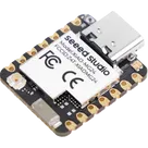
XIAO MG24 is an ultra-low-power wireless development board based on Silicon Labs' EFR32MG24 SoC, featuring a high-performance 78MHz ARM Cortex®-M33 core. It‘s Matter® native over Thread® and Bluetooth® Low Energy 5.3, all supported by the Arduino® Core. With 4MB Flash onboard, 19 GPIOs, LED, and charging circuit, it boasts extremely low operating current and ultra-low-power modes, making it an ideal choice for IoT applications, especially battery-powered projects utilizing Matter® protocols.
This model is used for through holes dip-14 connectors instead of SMD.
Properties
Pricing & Availability
Distributor | Qty 1 |
|---|
Controls
Welcome 👋
Flux accelerates your PCB design with AI.
Create your account to start using this component and bring your ideas to life.