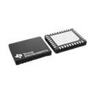
Part Metadata Review and Verification
Thought for 2 mins 35 sec
1. Part review
Available part metadata
Symbol/footprint structure found in the part project
Special features
Absolute maximum ratings
Recommended operating conditions
Selected electrical characteristics extracted
Package metadata
Package dimensions extracted
Pin descriptions
4. Symbol and footprint cross-check
What matches
Mismatches / risks
Bottom line
Table
| Field | Value |
|---|---|
| MPN | BQ25773REER |
| Manufacturer | Texas Instruments |
| Description | Battery Management IC, 2-cell to 5-cell NVDC dual-phase buck-boost battery charge controller with system power monitor |
| Datasheet | |
| Project package property | TO |
| Datasheet package | REE (WQFN, 36) |
| Datasheet body size | 4.00 mm x 5.00 mm |
| Datasheet max height | 0.8 mm |
| Symbol terminal count in project | 37 |
| Footprint pad count in project | 37 |
| 3D model | Present |
- The symbol contains 37 terminals: 36 numbered pins + 1 exposed pad.
- The footprint contains 37 pads: 36 perimeter pads + 1 large center pad.
- The center pad is assigned to PGND, which matches the datasheet’s Bottom pad (PGND) requirement.
- A datasheet URL is already set on the part.
- Because it already exists, no web search or property update was needed.
Table
| Category | Summary |
|---|---|
| Device type | Synchronous NVDC buck-boost battery charge controller |
| Battery support | 2-cell to 5-cell |
| Input source support | USB adapter, USB-C PD SPR, USB-C PD EPR, traditional adapters |
| Input operating range | 3.5 V to 40 V |
| Charge current | Up to 16.3 A / 30 A based on 5 mOhm / 2 mOhm sense resistor |
| Input current limit | Up to 8.2 A / 16.4 A based on 10 mOhm / 5 mOhm sense resistor |
| OTG | 3 V to 5 V, up to 3 A based on 10 mOhm sense resistor |
| Switching frequency | 600 kHz / 800 kHz programmable |
| Interface | I2C |
| ADC | Integrated 16-bit ADC |
| Accuracy | ±0.5% charge voltage regulation, ±2% charge current regulation, ±2% input current regulation, ±2% input/charge current monitor |
Table
| Feature | Notes |
|---|---|
| NVDC architecture | System stays regulated and can keep operating even if battery is discharged or removed |
| Quasi dual phase buck-boost | Seamless transition between buck, buck-boost, and boost |
| Pass Through Mode | Claimed >99% efficiency |
| DRSS | Dual random spread spectrum for EMI performance |
| ICO | Input Current Optimizer |
| FRS | Integrated Fast Role Swap for USB-PD |
| Intel platform support | IMVP8 / IMVP9 features including VAP and PROCHOT behavior |
| PSYS | System power monitor output |
| Protection | Thermal regulation, thermal shutdown, input/system/battery OVP, MOSFET and inductor OCP |
Table
| Parameter | Range |
|---|---|
| ACN_A, ACP_A, ACN_B, ACP_B, VBUS, VSYS | -0.3 V to 45 V |
| SW1_A, SW1_B, SW2 | -2 V to 45 V |
| SRN, SRP | -0.3 V to 30 V |
| BATDRV | -0.3 V to 35 V |
| BTST1_A, BTST1_B, HIDRV1_A, HIDRV1_B | -0.3 V to 50 V |
| BTST2, HIDRV2 | -0.3 V to 50 V |
| LODRV1_A, LODRV1_B, LODRV2 (25 ns) | -4 V to 5.5 V |
| HIDRV1_A, HIDRV1_B (25 ns) | -4 V to 50 V |
| HIDRV2 (25 ns) | -4 V to 50 V |
| SW1_A, SW1_B (25 ns) | -4 V to 45 V |
| SW2 (25 ns) | -4 V to 45 V |
| SDA, SCL, REGN_A, REGN_B, CHRG_OK, CELL_BATPRES, ILIM_HIZ, LODRV1_A, LODRV1_B, LODRV2, CMPIN_TR, CMPOUT, MODE, EN_OTG | -0.3 V to 5.5 V |
| /PROCHOT | -0.3 V to 5.5 V |
| IADPT, IBAT, PSYS | -0.3 V to 3.6 V |
| BTST1_A-SW1_A, BTST1_B-SW1_B, BTST2-SW2, HIDRV1_A-SW1_A, HIDRV1_B-SW1_B, HIDRV2-SW2, BATDRV-SRP | -0.3 V to 5.5 V |
| SRP-SRN, ACP_A-ACN_A, ACP_B-ACN_B | -0.3 V to 0.3 V |
| Junction temperature | -40 C to 150 C |
| Storage temperature | -55 C to 150 C |
Table
| Parameter | Range |
|---|---|
| ACP_A, ACN_A, ACP_B, ACN_B, VBUS | 0 V to 40 V |
| VSYS | 0 V to 23 V |
| SRP, SRN | 0 V to 23 V |
| SW1_A, SW1_B | -2 V to 40 V |
| SW2 | -2 V to 23 V |
| BTST1_A, BTST1_B, HIDRV1_A, HIDRV1_B | 0 V to 45 V |
| BTST2, HIDRV2, BATDRV | 0 V to 28 V |
| SDA, SCL, REGN_A, REGN_B, CHRG_OK, CELL_BATPRES, ILIM_HIZ, LODRV1_A, LODRV1_B, LODRV2, CMPIN_TR, CMPOUT, MODE, EN_OTG | 0 V to 5.3 V |
| /PROCHOT | 0 V to 5 V |
| IADPT, IBAT, PSYS | 0 V to 3.3 V |
| Differential: BTSTx-SWx, HIDRVx-SWx, BATDRV-SRP | 0 V to 5 V |
| Differential: SRP-SRN, ACP_A-ACN_A, ACP_B-ACN_B | -0.2 V to 0.2 V |
| Junction temperature | -40 C to 125 C |
Table
| Parameter | Value |
|---|---|
| Input voltage operating range | 3.5 V to 40.00 V |
| System voltage regulation range | 5.16 V to 23.16 V |
| Charge current regulation accuracy | -1.5% to 1.5% |
| REGN overvoltage falling threshold | 5.10 V / 5.30 V / 5.50 V min/typ/max |
| HIZ battery-powered current | 1000 uA / 1150 uA typ/max |
| PSYS gain accuracy | -3.5% to 2% |
| PSYS clamp voltage | 3.1 V / 3.3 V |
| System OVP rising threshold, 2s | 11.85 V / 12.15 V / 12.35 V |
| System OVP rising threshold, 3s | 16.8 V / 17.15 V / 17.4 V |
| System OVP rising threshold, 4s | 21.90 V / 22.3 V / 22.60 V |
| Comparator threshold | 1.18 V / 1.2 V / 1.23 V |
| EN_OTG low input | 0.8 V |
| EN_OTG high input | 1.35 V |
| I2C low input threshold | 0.42 V |
Table
| Field | Value |
|---|---|
| Orderable part | BQ25773REER |
| Status | Active Production |
| Package | WQFN (REE) |
| Pin count | 36 pins |
| Body size | 4.00 mm x 5.00 mm |
| Height | 0.8 mm max |
| Lead finish | NIPDAU |
| MSL | Level-1-260C-UNLIM |
| Operating temperature | -40 C to 125 C |
| Part marking | BQ25773 |
Table
| Dimension | Value |
|---|---|
| Body A | 3.9 mm to 4.1 mm |
| Body B | 4.9 mm to 5.1 mm |
| Max height | 0.8 mm |
| Lead width | 0.15 mm to 0.25 mm |
| Lead length | 0.3 mm to 0.5 mm |
| Pin pitch | 0.4 mm |
| Thermal pad | 2.6 mm to 2.8 mm |
| Datasheet land-pattern exposed pad | 3.6 mm x 2.8 mm |
Table
| Pin | Project terminal | Datasheet description |
|---|---|---|
| 1 | LODRV1_A | Buck phase A low-side MOSFET driver output |
| 2 | REGN_A | 5 V LDO output for gate drive; requires 2.2 uF or 3.3 uF ceramic capacitor to power ground |
| 3 | BTST1_A | Bootstrap supply for phase A high-side driver; connect 0.1 uF between SW1_A and BTST1_A |
| 4 | HIDRV1_A | Buck phase A high-side MOSFET driver |
| 5 | SW1_A | Buck phase A switching node |
| 6 | VBUS | Charger input voltage; recommends 1 ohm + 0.47 uF min input low-pass filter |
| 7 | ACN_B | Phase B input current-sense negative input; RC filter required |
| 8 | ACP_B | Phase B input current-sense positive input; RC filter required |
| 9 | ACN_A | Phase A input current-sense negative input; RC filter required |
| 10 | ACP_A | Phase A input current-sense positive input; RC filter required |
| 11 | CHRG_OK | Open-drain status output; use 10 kOhm pullup |
| 12 | EN_OTG | Active-high OTG / VAP / FRS enable input |
| 13 | ILIM_HIZ | Input current-limit programming pin via resistor divider |
| 14 | IADPT | Adapter current monitor output |
| 15 | IBAT | Battery current monitor output |
| 16 | MODE | Operation mode pin; pull-down resistor required |
| 17 | PSYS | System power monitor output; resistor to ground generates voltage; clamp near 3.2 V |
| 18 | ~PROCHOT | Active-low open-drain processor hot output |
| 19 | SDA | I2C data, open-drain; use 10 kOhm pullup |
| 20 | SCL | I2C clock input; use 10 kOhm pullup |
| 21 | CMPOUT | Open-drain comparator output |
| 22 | CMPIN_TR | Comparator input / temperature regulation input; tie to ground if unused |
| 23 | CELL_BATPRES | Cell-count and battery-present pin via resistor divider; no external capacitor allowed |
| 24 | SRN | Battery current-sense negative input and battery voltage sense; use 0.1 uF filter cap across sense resistor and 10 ohm contact resistor |
| 25 | SRP | Battery current-sense positive input; use 0.1 uF filter cap across sense resistor |
| 26 | BATDRV | BATFET gate driver output |
| 27 | VSYS | Charger system voltage sense |
| 28 | SW2 | Boost switching node |
| 29 | HIDRV2 | Boost high-side MOSFET driver |
| 30 | BTST2 | Bootstrap supply for boost high-side driver; connect 0.1 uF between SW2 and BTST2 |
| 31 | LODRV2 | Boost low-side MOSFET driver |
| 32 | REGN_B | 5 V LDO output; internally connected to REGN_A; requires 2.2 uF or 3.3 uF capacitor |
| 33 | LODRV1_B | Buck phase B low-side MOSFET driver |
| 34 | BTST1_B | Bootstrap supply for phase B high-side driver; connect 0.1 uF between SW1_B and BTST1_B |
| 35 | HIDRV1_B | Buck phase B high-side MOSFET driver |
| 36 | SW1_B | Buck phase B switching node |
| Exposed pad | PGND | Common power ground thermal pad; must be soldered and tied into PGND with multiple vias |
Table
| Check | Result |
|---|---|
| Pin naming | Looks consistent between symbol and footprint |
| Pin numbering | Looks consistent for the pins sampled against the datasheet |
| Total connection count | Looks consistent: 36 pins + exposed pad |
| Exposed pad function | Looks consistent: center pad is mapped to PGND |
| Package family / size | Looks broadly consistent with a 4 mm x 5 mm WQFN with exposed pad |
Table
| Severity | Issue | Why it matters |
|---|---|---|
| High | The project property Package or Case Code = TO does not match the datasheet package REE (WQFN, 36) | This can cause incorrect ordering metadata, bad library search matches, or confusion during manufacturing handoff |
| Medium | The footprint uses a center pad around 2.8 mm x 3.8 mm, while the datasheet extracts indicate thermal-pad related dimensions of 2.6 mm to 2.8 mm for package pad and 3.6 mm x 2.8 mm for land pattern | This should be manually verified because exposed-pad geometry directly affects soldering, thermal performance, and assembly yield |
| Medium | The footprint asset naming implies a generic 37-pad QFN pattern rather than explicitly the TI REE0036A package code | It may still be correct, but it increases the chance of an almost-right footprint being used for the wrong package revision |
| Medium | The datasheet explicitly requires the exposed pad to be soldered and tied into PGND with multiple vias | If the final footprint or recommended layout omits via-ready thermal strategy, the device may suffer thermal and mechanical reliability issues |
- Symbol: no obvious pin-name or pin-count problem found.
- Footprint: mostly plausible, but the package metadata is definitely wrong and the exposed-pad / land-pattern dimensions should be verified against TI REE0036A before release.
If you want, I can next turn this into a concise fix list for the part project, ordered by manufacturing risk.
Make a fix list
Check exposed pad
Review symbol pins