Part Review and Datasheet Verification
Thought for 5 mins 29 sec
Here’s a complete review of the part project for ADPD144RI-ACEZ-RL7, executed in the requested order.
- Review of available part information (as currently set in the project)
- MPN: ADPD144RI-ACEZ-RL7
- Description: not set (project description shows “ADPD144RI-ACEZ-RL7 / CE-12-2_ADI CE-12-2_ADI-M CE-12-2_ADI-L”)
- Designator Prefix: U
- Datasheet: https://www.analog.com/media/en/technical-documentation/data-sheets/ADPD144RI.pdf
- Package: not explicitly set in project properties
- Pin count: 12 symbol pins present in the schematic via terminals
- Datasheet URL check and update
- A datasheet URL is already set on the part. No changes required.
- Datasheet scan and metadata extraction (ADPD144RI.pdf)
Features (exact items)
- 2.8 mm × 5.0 mm module with integrated optical components
- 660 nm LED, 880 nm IR LED, and photodiode
- Fully integrated AFE, ADC, LED drivers, and timing core
- Custom optical package for use under a glass window
- Programmable 2-channel, 8.5 mA to 370 mA LED drivers
- Provision to use external LED emitters
- Low power
- Specifically designed for ultralow direct optical reflections
- Independent AFE settings per channel
- I2C data and control interface
- Burst accumulator enabling 20 bits per sample period
- Sample to sample accumulator enabling up to 27 bits per data read
- 16-bit or 32-bit register or FIFO readout per channel
Applications
- Optical heart rate monitoring
- Reflective SpO2 measurement
Recommended operating conditions
- VDD (VDD1 and VDD2): min 1.7 V, typ 1.8 V, max 1.9 V
- VLED (LED anode supply): min 3.0 V, typ 3.5 V, max 4.3 V
- Operating temperature range: −40 to +85 °C
Selected electrical characteristics
- Power supply current (VDD1, VDD2 = 1.8 V)
- Peak supply current (4-channel operation): 9.3 mA
- Standby mode current: 3.5 µA
- Example average supply current (depend on configuration; references provided in table):
- 1 pulse @100 Hz, Time Slot A only: 106 µA
- 1 pulse @100 Hz, Time Slot B only: 94 µA
- 1 pulse @100 Hz, A+B: 151 µA
- 10 pulses @100 Hz, A only: 258 µA
- 10 pulses @100 Hz, B only: 246 µA
- 10 pulses @100 Hz, A+B: 455 µA
- VLED supply current, average (peak LED current 100 mA, 3 µs pulse)
- 1 pulse: 50 Hz 15 µA; 100 Hz 30 µA; 200 Hz 60 µA
- 10 pulses: 50 Hz 150 µA; 100 Hz 300 µA; 200 Hz 600 µA
- LEDs
- LED peak current setting: 8.5 mA to 370 mA (programmable)
- Dominant wavelength: Red (LED1) 660 nm; IR (LED2) 880 nm
- Radiant flux (typ): Red 9 mW at IF = 20 mA; IR 33 mW at IF = 100 mA
- Photodiode
- Responsivity (typ): 660 nm: 0.36 A/W (Ch1–3), 0.31 A/W (Ch4); 880 nm: 0.25 A/W (Ch1–3), 0.28 A/W (Ch4)
- Active area: 0.3 mm² (individual), 1.2 mm² (total)
- Power supply
- PSRR at VDD = 1.8 V: −37 dB
- Data acquisition
- ADC resolution (single pulse): 14 bits
- Output data width: up to 27 bits (per table conditions)
- Sampling frequency: 0.122 Hz (lowest) to 3.48 kHz (Time Slot B, one pulse/sample, tSLEEP = 200 µs)
- Minimum sleep time: 200 µs
Absolute maximum ratings
- A dedicated “Absolute Maximum Ratings” table was not found in the datasheet. Only recommended operating conditions and specifications are provided.
Pin configuration and descriptions
Pin mapping (from Table 8)
- 1 — LGND — Supply — LED Ground.
- 2 — SDA — Digital input and output — Serial Address and Data.
- 3 — DGND — Supply — Digital Ground.
- 4 — AGND — Supply — Analog Ground.
- 5 — VDD1 — Supply — 1.8 V Supply Input.
- 6 — VREF — Analog reference — Voltage Reference. Bypass with a 0.7 µF to 4 µF capacitor to AGND. Recommended value is 1 µF.
- 7 — VLED — Supply — Integrated LEDs Anode Supply Voltage.
- 8 — LEDX2 — Analog output — External LED2 Cathode. Do not connect this pin unless driving external LEDs.
- 9 — LEDX1 — Analog output — External LED1 Cathode. Do not connect this pin unless driving external LEDs.
- 10 — VDD2 — Supply — 1.8 V Supply Input.
- 11 — INT — Digital input and output — Interrupt Input and Output.
- 12 — SCL — Digital input — Serial Clock for I2C Communication.
Package and land pattern
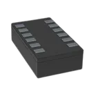
- Package description: 12-Terminal Chip Array Small Outline No Lead Cavity [LGA_CAV]
- Body size: 2.8 mm × 5.0 mm
- Package option code: CE-12-2
- Land Pattern (recommended): Figure 20 (datasheet) shows recommended PCB footprint with callouts including 0.905 mm, 0.7 mm, 0.45 mm, and 2.0 mm dimensions, along with the 12-pin numbering layout.
Ordering guide
- ADPD144RI-ACEZ-RL7 — −40 °C to +85 °C — 12-Terminal LGA_CAV — CE-12-2 — 7” tape and reel
- ADPD144RI-ACEZ-RL — −40 °C to +85 °C — 12-Terminal LGA_CAV — CE-12-2 — 13” tape and reel
- Cross-check: schematic symbol and footprint vs datasheet
Schematic symbol vs datasheet
- Pin count: 12 pins present in symbol; matches datasheet (12-terminal LGA_CAV).
- Pin names and numbers: Match datasheet exactly (verified one-to-one):
- Pin electrical types in the symbol:
Footprint vs datasheet
- Footprint present: 8b17a09e-fef0-4805-b4be-89e6ed5fded6.defaultFootprint with 12 pads (LGND, SDA, DGND, AGND, VDD1, VREF, VLED, LEDX2, LEDX1, VDD2, INT, SCL) — count matches package.
- Footprint source/identity: Asset name “CE-12-2_ADI.kicad_mod”; footprint text tag “ADPD144RI-ACEZ-RL7”; package label “CE-12-2_ADI” — aligns with datasheet package option CE-12-2.
- Pin 1 indicator: Present (F.SilkS circle at lower-left), consistent with typical orientation for pad “1”.
- Body outline (F.Fab): 2.8956 mm × 5.1054 mm nominal rectangle; consistent with a 2.8 mm × 5.0 mm body callout (slight drafting margin on fab layer is typical).
- Pad geometry from footprint:
- Pads per side: 6 per side, total 12
- Y-pitch: approximately 0.70 mm between adjacent pads
- Pad size: 0.6604 mm × 0.4572 mm
- Row-to-row center spacing: approximately 2.032 mm (pad centers at ±1.016 mm)
- Land pattern conformance:
- Datasheet land pattern figure (Figure 20) shows callouts including 0.7 mm (pitch), 0.45 mm (pad width), and 2.0 mm (row spacing), which are consistent with the footprint’s 0.70 mm pitch, 0.4572 mm width, and ~2.032 mm spacing.
- The datasheet also shows a 0.905 mm callout in the land pattern figure; confirm whether this refers to pad length or an offset. The footprint uses 0.6604 mm pad length. If the 0.905 mm dimension is the recommended pad length, this is a potential mismatch; if it denotes another spacing, the footprint may be correct. Recommend verifying the figure’s legend against the current pad length.
Actionable flags and recommendations
- Update pin types for grounds:
- Verify land pattern pad length:
- Compare the datasheet’s 0.905 mm callout in Figure 20 to the footprint’s pad length 0.6604 mm. If 0.905 mm is the recommended pad length, adjust pads accordingly; otherwise, document the interpretation used when generating the footprint.
- Ensure VREF decoupling guidance is captured:
- Datasheet requires 0.7 µF to 4 µF to AGND (1 µF recommended). Consider adding a property/note in the part description or a reference design note to prevent omission in schematics.
- Everything else checks out:
- Pin names, numbers, functions, and symbol-to-footprint mapping align with the datasheet.
- Package identity and count match the ordering guide (CE-12-2, 12-terminal LGA_CAV).
- Pin 1 indicator present and consistent.
If you want, I can fix the ground pin types and, if desired, adjust the footprint pad length after you confirm the intended interpretation of the 0.905 mm land pattern dimension.
Fix ground pin types
Check pad length callout
Add VREF capacitor note
Run DRC/ERC review