Part Project Datasheet Review
Thought for 3 mins 28 sec
Here’s a complete, tool-backed review of your part project, executed in order.
- Review of available part information
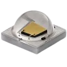
- Project MPN: XPEBRD-L1-0000-00701 (CREE LED)
- Description: LED Lighting Color XLamp XP‑E2 Red 625 nm (620 nm ~ 630 nm) 1414 (3535 Metric)
- Part type: Optoelectronic Devices
- Designator prefix: LED
- Schematic symbol pins (count = 3):
- Footprint summary (from embedded footprint rules):
- Package outline: 3.45 mm x 3.45 mm (F.Fab square: ±1.725 mm), courtyard ±2.725 mm
- Pads (top, SMD):
- Pad 1: 0.500 mm x 3.300 mm at x = -1.400 mm
- Pad 2: 0.500 mm x 3.300 mm at x = +1.400 mm
- Pad 3 (center thermal): 1.300 mm x 3.300 mm at x = 0.000 mm
- Silkscreen: small arc marker at left (around x ≈ -2.25 mm)
- 3D model: XPEBRD-L1-0000-00701.stp
- Datasheet presence
- Datasheet: Datasheet is already set. No update needed.
- Datasheet scan and metadata extraction (XLamp XP‑E2) Special features
- Available colors include red; ANSI-compatible bins; wide viewing angle; electrically neutral thermal path; RoHS/REACH; JEDEC reflow compatible; UL recognized component.
- Maximum drive current: royal blue/blue 1.2 A; others (including red) 1.5 A.
Absolute maximum ratings and limits
- Maximum DC forward current (red): 1500 mA.
- LED junction temperature (max): 150 °C.
- Reverse voltage (red): 1 V.
- ESD classification (HBM per MIL‑STD‑883D): Class 3B.
- Reflow profile (lead-free, JEDEC J‑STD‑020C compatibility):
- Ramp-up (Tsmax to Tp): 1.2 °C/s
- Preheat: 120–170 °C for 65–150 s
- Above liquidus (217 °C): 45–90 s
- Peak/classification temp (Tp): 235–245 °C
- Within 5 °C of peak: 20–40 s
- Ramp-down: 1–6 °C/s
- 25 °C to peak: 4 min max.
- Moisture sensitivity: MSL 1 (unlimited floor life at ≤ 30 °C / 85% RH).
Recommended operating characteristics (red)
- Forward current range: 0 to 1500 mA (datasheet curves shown over this range).
- Viewing angle (FWHM): 130° (red).
- Thermal resistance, junction-to-solder point (red/red-orange/photo red): 2.5 °C/W.
- Electrical characteristics (typical values at 25 °C where provided):
- VF @ 350 mA (red): typical 2.08 V, maximum 2.6 V.
- VF @ 1000 mA (red): ~2.44 V (typical).
- Optical (examples from luminous flux bins at 350 mA, red):
- P2: ≥ 67.2 lm; P3: ≥ 73.9 lm; P4: ≥ 80.6 lm.
- Wavelength (dominant) bins for red:
- R2: 620–625 nm; R3: 625–630 nm.
- Thermal path: Electrically neutral thermal path (center pad) intended for heat conduction.
Package dimensions and land pattern
- Package outline: 3.45 mm × 3.45 mm.
- Datasheet provides Recommended PCB Footprint and Recommended Stencil Opening (numeric values are shown graphically in the datasheet drawings).
- Polarity identification:
- Top view: “CATHODE SIDE” is on the left; “ANODE SIDE” on the right.
- Bottom view: “ANODE SIDE” is the left pad; “CATHODE SIDE” is the right pad.
- The datasheet identifies side/polarity by drawing labels rather than an explicit “cathode dot” callout.
- Cross‑check: schematic symbol and footprint vs datasheet Schematic symbol
- Pins present and named: K, A, EP. Count = 3. This matches the XP‑E2: anode, cathode, and center thermal pad.
- Pin numbering: K=1, A=2, EP=3 in symbol properties. This aligns with a 3‑pad LED plus thermal pad mapping.
- Pin types are set to “Unspecified”. Recommendation: set K and A to “Passive”; set EP to “Passive” with a note “Thermal only; electrically neutral path per datasheet.”
Footprint and mapping
- Pad count and sizes: 3 pads total; two narrow outer pads (0.5 x 3.3 mm) and one larger center thermal pad (1.3 x 3.3 mm). This is consistent with XP‑E2 style packages.
- Package outline: F.Fab square at ±1.725 mm confirms a 3.45 mm square body per datasheet.
- Polarity/marker: Silkscreen arc at left; datasheet indicates cathode side is left (top view). This is appropriate as a left-side orientation mark.
- Pad numbering vs symbol numbering:
- Footprint pads are numbered 1 (left), 2 (right), 3 (center).
- Symbol pin numbers are 1=K (left/cathode), 2=A (right/anode), 3=EP (center).
- This mapping matches datasheet polarity conventions (left=cathode, right=anode).
- Thermal pad function: Datasheet states an “electrically neutral thermal path.” Ensure EP (pad 3) is not tied to an electrical net unless your design intent requires it; typically it should be connected to a thermal copper region with vias for heat spreading, not to a signal net.
- Land pattern dimensions: The embedded footprint provides concrete pad sizes and spacing. The datasheet provides a recommended land pattern; while numeric values were not surfaced in text search, the general geometry and package dimensions match. Action to consider: visually confirm pad dimensions against the datasheet’s “Recommended PCB Footprint” drawing to validate exact values.
Potential issues or mismatches to address
- Schematic pin electrical types are “Unspecified.” Consider setting:
- K: Passive
- A: Passive
- EP: Passive (thermal only; add property note referencing datasheet’s “electrically neutral thermal path”).
- Verify that your symbol-to-footprint pin mapping is explicitly K -> Pad 1, A -> Pad 2, EP -> Pad 3 in the part definition. The current numbering and silkscreen suggest it is correct; double-check the mapping table in the part to prevent assembly polarity errors.
- If your assembly requires explicit polarity marking on silkscreen, the left-side arc is good, but consider adding a clear cathode indicator per your fab house marking conventions.
If you want, I can update the pin types and add a note to EP, or adjust the footprint silkscreen/pin mapping after confirming your preferences.
@review manufacturing checks
@help edit pin types
@layout inspect pad mapping
@file verify land pattern