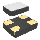
Part Datasheet Review and Updates
Worked for 4 mins 8 sec
I reviewed the part project against its datasheet and the current symbol/footprint setup. I followed the standard part-project sync workflow: verify the datasheet URL first, then compare project metadata, terminals, and footprint against the datasheet pinout and package data
Result
- The
Datasheet URLproperty is already set, so no web lookup or property update was needed. - The project has the correct 4-terminal structure for this crystal.
- The footprint pin numbering and pad geometry match the datasheet land pattern.
- I found metadata mismatches and missing terminal details that should be corrected.
Table
| Property | Current value | Status |
|---|---|---|
| Manufacturer Part Number | CX3225SB16000D0GZJC1 | OK |
| Manufacturer Name | KYOCERA | Slight mismatch |
| Part Type | Crystals and Oscillators | Acceptable but broad |
| Datasheet URL | Set | OK |
| Designator Prefix | Y | OK |
Table
Table
| Item | Datasheet value |
|---|---|
| Manufacturer | KYOCERA Crystal Device Corporation |
| MPN | CX3225SB16000D0GZJC1 |
| Device type | Quartz crystal |
| Package | 3.2 mm × 2.5 mm, 4-pad SMD |
| Frequency | 16 MHz |
| Load capacitance | 8.0 pF |
| Frequency tolerance | ±15 ppm at +25 ±3 °C |
| Frequency temp characteristic | ±15 ppm over operating range |
| ESR | 60 Ω max |
| Drive level | 10 µW typ, 100 µW max |
| Insulation resistance | 500 MΩ min at 100 VDC |
| Operating temperature | -10 °C to +75 °C |
| Storage temperature | -40 °C to +85 °C |
| Aging | ±1 ppm/year first year |
Table
| Pin | Datasheet function | Recommended Flux pin type |
|---|---|---|
| 1 | HOT | Passive |
| 2 | GND | Ground |
| 3 | HOT | Passive |
| 4 | GND | Ground |
The datasheet explicitly lists the layout as #1 HOT, #2 GND, #3 HOT, #4 GND, which matches the existing project numbering. For simple crystal parts, the pin-type mapping should follow the standard passive/ground treatment rather than leaving terminals as
Footprint verification
Datasheet recommended land pattern
UnspecifiedTable
| Parameter | Value |
|---|---|
| Pad size | 1.05 mm × 1.30 mm |
| Horizontal pad pitch | 2.30 mm |
| Vertical pad pitch | 1.85 mm |
| Body size | 3.20 mm × 2.50 mm |
The project footprint asset
CX3225SB16000D0GZJC1.kicad_mod contains:Table
| Pad | Position (mm) | Size (mm) | Rotation |
|---|---|---|---|
| 1 | (-1.150, 0.925) | 1.050 × 1.300 | 90° |
| 2 | (1.150, 0.925) | 1.050 × 1.300 | 90° |
| 3 | (1.150, -0.925) | 1.050 × 1.300 | 90° |
| 4 | (-1.150, -0.925) | 1.050 × 1.300 | 90° |
Derived spacing:
- Horizontal center-to-center: 2.300 mm
- Vertical center-to-center: 1.850 mm
- Pad count: match
- Pad numbering: match
- Pad sizes: match
- Pad spacing: match
- Body outline: consistent with 3.2 mm × 2.5 mm
So the PCB footprint looks correct against the datasheet.
Mismatches and issues found
1) Operating temperature in the project description is wrong
Your project description says:
−25°C to +85°C
But the datasheet says:
- Operating:
-10°C to +75°C - Storage:
-40°C to +85°C
So the description appears to have mixed up storage and operating limits.
2) Manufacturer name is not exact
Current property:
KYOCERA
Datasheet name:
KYOCERA Crystal Device Corporation
Not critical, but it is a metadata mismatch.
3) Part Type is broader than necessary
Current:
Crystals and Oscillators
Datasheet describes this specifically as:
- Quartz crystal
Not wrong, but less precise than it could be.
4) Terminal pin types are incomplete
All four terminals are currently
Unspecified.Recommended:
5) Terminal descriptions are missing
Each terminal should have a short description, for example:
Summary
What is correct
Table
| Area | Verdict |
|---|---|
| MPN | Correct |
| Datasheet URL | Present and valid |
| Pin count | Correct at 4 |
| Pin numbering | Correct |
| Footprint geometry | Matches datasheet |
Designator prefix Y | Correct |
Table
| Area | Recommended correction |
|---|---|
| Manufacturer Name | Change to KYOCERA Crystal Device Corporation |
| Project description | Replace temperature range with the correct operating range |
| Part Type | Optionally refine to Quartz crystal |
| Terminal pin types | Set HOT pins to Passive, GND pins to Ground |
| Terminal descriptions | Add short pin descriptions |
If you want, I can make those metadata and terminal-property fixes for you now.
Fix all mismatches
Check power parts first
Use official datasheets
Include BOM impact