PCB Design for Cinema Camera Power Distribution
0:00
- Replaced the temporary/incorrect ground tie path by removing R18 and adding SJ1 as a bridged solder-jumper intended for the single PGND-SGND star point.
- Added external I/O ESD protection: D5 and D6 are PESD3V3L5UY 5-channel 3.3V ESD arrays, wired to SMBUS, tally, timecode, genlock, CTRL, and V-mount SMBUS output nets.
- Wired D4 BAT54 as a clamp from SW_MAIN_BUS to PGND, matching the TPS26600 datasheet guidance for output negative-transient protection.
- Removed the stray SW_ENCODER_1 artifact; R18 was also removed.
- ✅ Added missing external-signal ESD protection.
- ✅ Added a proper star-point component (SJ1) for the PGND/SGND split.
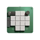
- ✅ Removed one known stray macro-keyboard artifact (SW_ENCODER_1).
- ⚠️ The SGND rename/tie still needs one follow-up pass: the tool rejected the SGND-side connection because the renamed SGND net was not available during that batch, so SJ1:B and the ESD common anodes still need to be tied to the signal-ground net.
- ⚠️ PCB placement/routing, mounting-hole verification, high-current layout rules, and final DRC/ERC remediation remain incomplete.
Started implementing a plan
Goal: Complete the RED KOMODO-X Power IO Distribution PCB (75x66mm, 2-layer, 2oz) providing dual-input ORing, protected main bus, fused aux bus, 3.3V logic rail, SMBUS filtering, tally output, pass-through IO, and edge solder pads, with proper PGND/SGND split and single star connection.
What is done so far:
- Project renamed and description updated to match KOMODO-X power/IO distribution board.
- Project specification doc created/updated in-project (size, stackup intent, edge pads only, ORing, TPS26600 eFuse, aux PTC, 3V3 LDO, SMBUS filtering, tally, PGND/SGND star).
- Schematic rebuilt around key power/IO blocks; major ICs placed and largely wired: U1 LTC4412 + Q1/Q2 AO3401A ideal-diode ORing, U2 TPS26600 eFuse feeding SW_MAIN_BUS, F1 MF-R1100 feeding AUX_6A_BUS, U3 AMS1117-3.3 generating 3V3_LOGIC, SMBUS beads FB1/FB2 plus pullups/series resistors, tally MOSFET Q3 SI2302 + LED indicators, TVS D1/D2/D3.
- Edge-pad components J1..J37 and TP1 created; many confirmed net assignments for power, grounds, SMBUS, tally, and pass-through signals.
- Board outline set to 75x66mm and 2-layer stackup selected.
- Added and wired improvements:
- Added SJ1 (Solder Jumper 2 Bridged) intended as PGND-to-SGND star element; removed prior incorrect R18 tie.
- Renamed prior unnamed logic ground net ("Net 1") is still pending correct conversion to SGND (rename operation failed due to net-creation rules).
- Added D5 and D6 (PESD3V3L5UY) ESD arrays and wired to multiple external IO nets; their common node still needs connection to SGND once SGND exists.
- Wired D4 BAT54 as SW_MAIN_BUS to PGND clamp (K to SW_MAIN_BUS, A to PGND).
- Removed stray SW_ENCODER_1; legacy "FLUX VECTOR PCB" likely still present in layout (removal attempt may not have succeeded).
- Review run indicates many airwires/unrouted connections; placement is out of bounds (many footprints outside board).
Implementation plan (remaining work only):
1. Create the SGND net properly and complete the PGND/SGND split: create SGND using a connect operation with newNetNameBase="SGND" (tie SJ1:B and all former logic-ground nodes), then verify SJ1 is the only intentional PGND<->SGND connection.
2. Reconnect ESD arrays D5/D6 common pin A to SGND, and verify each protected line (K1..K5) maps to the intended external nets; add/adjust any missing signal ESD channels if edge-pad count requires.
3. Audit and finish edge-pad net mapping for all J1..J37 and TP1 against the spec (VM B+, DC in, grounds, switched bus, aux bus, SMBUS in/out, tally, timecode/genlock/CTRL pass-through). Fix any pads left floating or misassigned.
4. Validate TPS26600 support network values and wiring per datasheet: set/confirm RILIM (R12), CdVdT (C14), UVLO/OVP divider resistors (R13/R14/R15/R16), MODE/RTN/GND/EP connections (ensure RTN is correct reference and not shorted to GND if reverse polarity protection is desired). Update component values/properties accordingly.
5. Review AMS1117 stability requirements: ensure output capacitor meets datasheet guidance (e.g., add/adjust to >=22uF with suitable ESR if needed) and confirm input/output capacitor placement intent on PCB.
6. Clean schematic/layout leftovers: confirm and remove any remaining macro-keyboard artifacts (including any lingering "FLUX VECTOR PCB" footprint/object), and mark intentional NC pins consistently.
7. Prepare layout for routing: confirm board corner radius/mechanical constraints (5mm inset mounting holes, edge-pad spacing), move/resize outline if needed, and ensure mounting hole positions match spec.
8. Place components within the 75x66mm outline using placement constraints: power input pads bottom edge; ORing + TPS26600 lower center; high-current bulk caps close to power path; LDO + SMBUS/IO upper half; SJ1 star point near lower-left input; keep edge pads on perimeter.
9. Define layout rules for high-current nets (VM_BPLUS, DC_IN_PLUS, OR_OUT_PROTECTED, SW_MAIN_BUS, AUX_6A_BUS, PGND) appropriate for 2oz copper; set clearances and via strategy.
10. Run autorouter for remaining nets, then add/confirm copper pours with split PGND and SGND regions and ensure they only connect via SJ1. Add stitching vias for PGND region as needed.
11. Re-run DRC/ERC (airwires, missing footprints, clearance) and iterate fixes until clean; then do manufacturability review (edge-pad DFM, trace widths, thermal reliefs, BOM sanity).
Execution stopped due to insufficient credits.
4:12
Thought for 5 sec
Read knowledge.
Read schematic.
Running design checks.
Read schematic.
Completed 6 design checks — found 193 issues.
Read U3 datasheet for AMS1117 output capacitor stability minim.
Read U3 datasheet for AMS1117 output capacitor stability minim.
Read U3 datasheet for AMS1117 output capacitor stability minim.
Read U2 datasheet for TPS26600 ILIM resistor equation current .
Read schematic.
Removed **, , , and 1 more**
0:02
Removed
Removed
Removed
Removed
Connected ^SGND
0:04
Connected SJ1:B, D5:A, D6:A to ^SGND
Connected ^TPS_RTN, disconnected 7 pins
0:02
Connected U2:RTN, R12:P2, C14:P2, R14:P2, R16:P2, R10:P2, U2:MODE to ^TPS_RTN
Disconnected U2:RTN, R12:P2, C14:P2, R14:P2, R16:P2, R10:P2, U2:MODE
Set Capacitance to "22uF" on C13, Set Voltage Rating to "10V" on C13, and 15 more changes
0:01
Set C13's Capacitance to "22uF"
Set C13's Voltage Rating to "10V"
Set C13's Role Details to "AMS1117 output stability capacitor, >=22uF placed close to VOUT and SGND"
Set C14's Capacitance to "22nF"
Set C14's Role to "Timing"
Set C14's Role Details to "TPS26600 dVdT capacitor from dVdT to RTN; 22nF gives controlled output ramp per TI example"
Set R12's Resistance to "5.36kohms"
Set R12's Tolerance to "1%"
Set R12's Role Details to "TPS26600 ILIM resistor to RTN; 5.36k sets maximum supported ~2.23A overload limit"
Set R13's Resistance to "715kohms"
Set R13's Tolerance to "1%"
Set R13's Role Details to "TPS26600 UVLO/OVP upper divider element for ~18V UVLO and ~30V OVP reference network"
Set R14's Resistance to "20kohms"
Set R14's Tolerance to "1%"
Set R14's Role Details to "TPS26600 UVLO/OVP middle divider element feeding UVLO node"
Set R15's Resistance to "30.1kohms"
Set R15's Tolerance to "1%"
Set R15's Role Details to "TPS26600 UVLO/OVP lower divider element feeding OVP node to RTN"
Set R16's Resistance to "0ohms"
Set R16's Role Details to "Placeholder/strap to tie OVP lower reference to TPS_RTN if using default/derived OVP scheme; verify against final divider top..."


Welcome 👋
Flux helps you build PCBs faster with an AI teammate!
Create your account to collaborate, stay updated, fork your own version, and get instant answers from our AI agent.